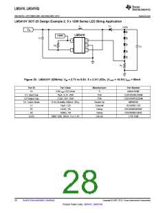
LM3410, LM3410Q
SNVS541G –OCTOBER 2007–REVISED MAY 2013
www.ti.com
'
≈ ’
D
IL2 =
x IL1
∆
÷
D
« ◊
and
D
= ≈ ’
IL1
∆
'÷ x
ILED
« D ◊
(58)
(59)
Substituting IL1 into IL2
IL2 = ILED
The average inductor current of L2 is the average output load.
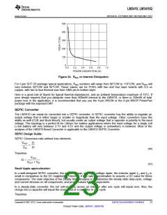
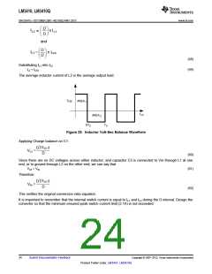
V
( )
AREA
1
L t
t
(s)
AREA
2
DT
T
S
S
Figure 25. Inductor Volt-Sec Balance Waveform
Applying Charge balance on C1:
'
(
)
VOUT
D
VC3
=
D
(60)
Since there are no DC voltages across either inductor, and capacitor C3 is connected to Vin through L1 at one
end, or to ground through L2 on the other end, we can say that
VC3 = VIN
(61)
Therefore:
'
(
)
VOUT
D
VIN =
D
(62)
This verifies the original conversion ratio equation.
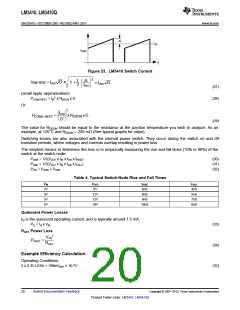
It is important to remember that the internal switch current is equal to IL1 and IL2 during the D interval. Design the
converter so that the minimum ensured peak switch current limit (2.1A) is not exceeded.
24
Submit Documentation Feedback
Copyright © 2007–2013, Texas Instruments Incorporated
Product Folder Links: LM3410 LM3410Q

 TI [ TEXAS INSTRUMENTS ]