LM2841, LM2842
SNVS540H –MARCH 2009–REVISED APRIL 2013
www.ti.com
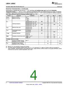
Electrical Characteristics (continued)
Specifications in standard type face are for TJ = 25°C and those with boldface type apply over the full Operating
Temperature Range ( TJ = −40°C to +125°C). Minimum and Maximum limits are specified through test, design, or statistical
correlation. Typical values represent the most likely parametric norm at TJ = +25°C, and are provided for reference purposes
only. Unless otherwise stated the following conditions apply: VIN = 12V.
(1)
(2)
(1)
Symbol
tON(min)
tOFF(min)
Parameter
Minimum ON time
Conditions
Min
Typ
100
Max
150
Units
ns
(6)
See
Minimum OFF time
X option
Y option
110
104
550
140
1.25
0.35
94
370
200
750
ns
ns
fSW
LM2840/41/42X, VFB = 0.5V
LM2840/41/42X, VFB = 0V
LM2840/41/42Y, VFB = 0.5V
LM2840/41/42Y, VFB = 0V
LM2840/41/42X
325
kHz
MHz
%
Switching frequency
Maximum duty cycle
0.95
1.50
DMAX
88
81
LM2840/41/42Y
87
VUVP
Undervoltage lockout
thresholds
On threshold
4.4
3.7
V
Off threshold
3.5
3.25
V SHDN
Shutdown threshold
Device on
2.3
1.0
V
Device off
0.9
0.3
1.5
1.5
(5)
ISHDN
Shutdown pin input bias current VSHDN = 2.3V
VSHDN = 0V
0.05
0.02
µA
THERMAL SPECIFICATIONS
(7)
RθJA
Junction-to-Ambient Thermal
See
121
94
°C/W
°C/W
Resistance, SOT-6L Package
RθJC
Junction-to-Case Thermal
Resistance, SOT-6L Package
(6) Minimum On Time specified by design and simulation.
(7) All numbers apply for packages soldered directly onto a 3" x 3" PC board with 2 oz. copper on 4 layers in still air in accordance to
JEDEC standards. Thermal resistance varies greatly with layout, copper thickness, number of layers in PCB, power distribution, number
of thermal vias, board size, ambient temperature, and air flow.
4
Submit Documentation Feedback
Copyright © 2009–2013, Texas Instruments Incorporated
Product Folder Links: LM2841 LM2842

 TI [ TEXAS INSTRUMENTS ]