LM2841, LM2842
SNVS540H –MARCH 2009–REVISED APRIL 2013
www.ti.com
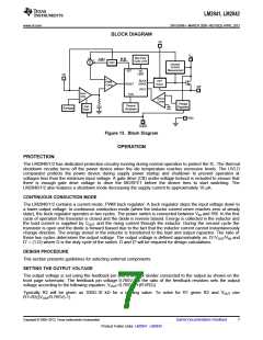
INPUT CAPACITOR
A low ESR ceramic capacitor (CIN) is needed between the VIN pin and GND pin. This capacitor prevents large
voltage transients from appearing at the input. Use a 2.2 µF-10 µF value with X5R or X7R dielectric. Depending
on construction, a ceramic capacitor’s value can decrease up to 50% of its nominal value when rated voltage is
applied. Consult with the capacitor manufacturer's data sheet for information on capacitor derating over voltage
and temperature.
INDUCTOR SELECTION
The most critical parameters for the inductor are the inductance, peak current, and the DC resistance. The
inductance is related to the peak-to-peak inductor ripple current, the input and the output voltages.
(VIN - VOUT)VOUT
L =
VIN x IRIPPLE x fSW
(1)
A higher value of ripple current reduces inductance, but increases the conductance loss, core loss, and current
stress for the inductor and switch devices. It also requires a bigger output capacitor for the same output voltage
ripple requirement. A reasonable value is setting the ripple current to be 30% of the DC output current. Since the
ripple current increases with the input voltage, the maximum input voltage is always used to determine the
inductance. The DC resistance of the inductor is a key parameter for the efficiency. Lower DC resistance is
available with a bigger winding area. A good tradeoff between the efficiency and the core size is letting the
inductor copper loss equal 2% of the output power. See AN-1197 SNVA038 for more information on selecting
inductors. A good starting point for most applications is a 10 µH to 22 µH with 1.1A or greater current rating for
the LM2842 or a 0.7A or greater current rating for the LM2840/41. Using such a rating will enable the
LM2840/1/2 to current limit without saturating the inductor. This is preferable to the LM2840/1/2 going into
thermal shutdown mode and the possibility of damaging the inductor if the output is shorted to ground or other
longterm overload.
OUTPUT CAPACITOR
The selection of COUT is driven by the maximum allowable output voltage ripple. The output ripple in the constant
frequency, PWM mode is approximated by: VRIPPLE = IRIPPLE(ESR+(1/(8fSWCOUT))) The ESR term usually plays
the dominant role in determining the voltage ripple. Low ESR ceramic capacitors are recommended. Capacitors
in the range of 22 µF-100 µF are a good starting point with an ESR of 0.1Ω or less.
BOOTSTRAP CAPACITOR
A 0.15 µF ceramic capacitor or larger is recommended for the bootstrap capacitor (CBOOT). For applications
where the input voltage is less than twice the output voltage a larger capacitor is recommended, generally 0.15
µF to 1 µF to ensure plenty of gate drive for the internal switches and a consistently low RDSON
.
SOFT-START COMPONENTS
The LM2840/1/2 has circuitry that is used in conjunction with the SHDN pin to limit the inrush current on start-up
of the DC/DC switching regulator. The SHDN pin in conjunction with a RC filter is used to tailor the soft-start for a
specific application. When a voltage applied to the SHDN pin is between 0V and up to 2.3V it will cause the cycle
by cycle current limit in the power stage to be modulated for minimum current limit at 0V up to the rated current
limit at 2.3V. Thus controlling the output rise time and inrush current at startup. The resistor value should be
selected so the current sourced into the SHDN pin will be greater then the leakage current of the SHDN pin (1.5
µA ) when the voltage at SHDN is equal or greater then 2.3V.
SHUTDOWN OPERATION
The SHDN pin of the LM2840/1/2 is designed so that it may be controlled using 2.3V or higher logic signals. If
the shutdown function is not to be used the SHDN pin may be tied to VIN. The maximum voltage to the SHDN pin
should not exceed 42V. If the use of a higher voltage is desired due to system or other constraints it may be
used, however a 100 kΩ or larger resistor is recommended between the applied voltage and the SHDN pin to
protect the device.
8
Submit Documentation Feedback
Copyright © 2009–2013, Texas Instruments Incorporated
Product Folder Links: LM2841 LM2842

 TI [ TEXAS INSTRUMENTS ]