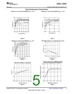
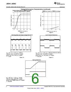
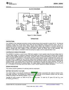
LM2841, LM2842
www.ti.com
SNVS540H –MARCH 2009–REVISED APRIL 2013
(1)(2)
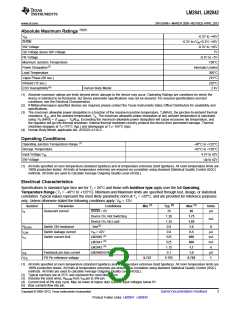
Absolute Maximum Ratings
VIN
-0.3V to +45V
SHDN
-0.3V to (VIN+0.3V) <45V
SW Voltage
-0.3V to +45V
7V
CB Voltage above SW Voltage
FB Voltage
-0.3V to +5V
150°C
Maximum Junction Temperature
Power Dissipation(3)
Lead Temperature
Vapor Phase (60 sec.)
Infrared (15 sec.)
Internally Limited
300°C
215°C
220°C
ESD Susceptibility(4)
Human Body Model
2 kV
(1) Absolute maximum ratings are limits beyond which damage to the device may occur. Operating Ratings are conditions for which the
device is intended to be functional, but device parameter specifications may not be ensured. For ensured specifications and test
conditions, see the Electrical Characteristics.
(2) If Military/Aerospace specified devices are required, please contact the Texas Instruments Sales Office/ Distributors for availability and
specifications.
(3) The maximum allowable power dissipation is a function of the maximum junction temperature, TJ(MAX), the junction-to-ambient thermal
resistance, θJA, and the ambient temperature, TA. The maximum allowable power dissipation at any ambient temperature is calculated
using: PD (MAX) = (TJ(MAX) − TA)/θJA. Exceeding the maximum allowable power dissipation will cause excessive die temperature, and
the regulator will go into thermal shutdown. Internal thermal shutdown circuitry protects the device from permanent damage. Thermal
shutdown engages at TJ=175°C (typ.) and disengages at TJ= 155°C (typ).
(4) Human Body Model, applicable std. JESD22-A114-C.
Operating Conditions
(1)
Operating Junction Temperature Range
Storage Temperature
Input Voltage VIN
−40°C to +125°C
−65°C to +150°C
4.5V to 42V
SW Voltage
Up to 42V
(1) All limits specified at room temperature (standard typeface) and at temperature extremes (bold typeface). All room temperature limits are
100% production tested. All limits at temperature extremes are ensured via correlation using standard Statistical Quality Control (SQC)
methods. All limits are used to calculate Average Outgoing Quality Level (AOQL).
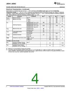
Electrical Characteristics
Specifications in standard type face are for TJ = 25°C and those with boldface type apply over the full Operating
Temperature Range ( TJ = −40°C to +125°C). Minimum and Maximum limits are specified through test, design, or statistical
correlation. Typical values represent the most likely parametric norm at TJ = +25°C, and are provided for reference purposes
only. Unless otherwise stated the following conditions apply: VIN = 12V.
(1)
(2)
(1)
Symbol
Parameter
Quiescent current
Conditions
SHDN = 0V
Min
Typ
16
Max
40
Units
IQ
µA
Device On, Not Switching
Device On, No Load
See(3)
1.30
1.35
0.9
1.75
1.85
1.6
mA
RDSON
ILSW
ICL
Switch ON resistance
Switch leakage current
Switch current limit
Ω
µA
mA
mA
A
VIN = 42V
0.0
0.5
(4)
LM2840
525
525
1.15
0.1
900
900
1.7
(4)
LM2841
(4)
LM2842
(5)
IFB
Feedback pin bias current
FB Pin reference voltage
LM2840/41/42
1.0
µA
V
VFB
0.747
0.765
0.782
(1) All limits specified at room temperature (standard typeface) and at temperature extremes (bold typeface). All room temperature limits are
100% production tested. All limits at temperature extremes are ensured via correlation using standard Statistical Quality Control (SQC)
methods. All limits are used to calculate Average Outgoing Quality Level (AOQL).
(2) Typical numbers are at 25°C and represent the most likely norm.
(3) Includes the bond wires, RDSON from VIN pin to SW pin.
(4) Current limit at 0% duty cycle. May be lower at higher duty cycle or input voltages below 6V.
(5) Bias currents flow into pin.
Copyright © 2009–2013, Texas Instruments Incorporated
Submit Documentation Feedback
3
Product Folder Links: LM2841 LM2842

 TI [ TEXAS INSTRUMENTS ]