LM2841, LM2842
www.ti.com
SNVS540H –MARCH 2009–REVISED APRIL 2013
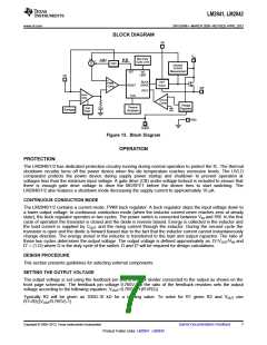
BLOCK DIAGRAM
CB
V
IN
Max Duty
Cycle Limit
+
+
OSC
Inductor
Current
Measurement
SET
DC
LIMIT
FB
+
BUCK
DRIVE
FET
Driver
PWM
Comp
-
RESET
TSD
SW
UVLO
-
Error
Amp
+
UVLO
Comp
Voltage
Regulator
Thermal
Shutdown
Soft
Start
Bandgap
BG
GND
SHDN
Figure 13. Block Diagram
OPERATION
PROTECTION
The LM2840/1/2 has dedicated protection circuitry running during normal operation to protect the IC. The thermal
shutdown circuitry turns off the power device when the die temperature reaches excessive levels. The UVLO
comparator protects the power device during supply power startup and shutdown to prevent operation at
voltages less than the minimum input voltage. A gate drive (CB) under-voltage lockout is included to ensure that
there is enough gate drive voltage to drive the MOSFET before the device tries to start switching. The
LM2840/1/2 also features a shutdown mode decreasing the supply current to approximately 16 µA.
CONTINUOUS CONDUCTION MODE
The LM2840/1/2 contains a current-mode, PWM buck regulator. A buck regulator steps the input voltage down to
a lower output voltage. In continuous conduction mode (when the inductor current never reaches zero at steady
state), the buck regulator operates in two cycles. The power switch is connected between VIN and SW. In the first
cycle of operation the transistor is closed and the diode is reverse biased. Energy is collected in the inductor and
the load current is supplied by COUT and the rising current through the inductor. During the second cycle the
transistor is open and the diode is forward biased due to the fact that the inductor current cannot instantaneously
change direction. The energy stored in the inductor is transferred to the load and output capacitor. The ratio of
these two cycles determines the output voltage. The output voltage is defined approximately as: D=VOUT/VIN and
D’ = (1-D) where D is the duty cycle of the switch. D and D' will be required for design calculations.
DESIGN PROCEDURE
This section presents guidelines for selecting external components.
SETTING THE OUTPUT VOLTAGE
The output voltage is set using the feedback pin and a resistor divider connected to the output as shown on the
front page schematic. The feedback pin voltage 0.765V, so the ratio of the feedback resistors sets the output
voltage according to the following equation: VOUT=0.765V(1+(R1/R2))
Typically R2 will be given as 100Ω-10 kΩ for a starting value. To solve for R1 given R2 and VOUT use
R1=R2((VOUT/0.765V)-1).
Copyright © 2009–2013, Texas Instruments Incorporated
Submit Documentation Feedback
7
Product Folder Links: LM2841 LM2842

 TI [ TEXAS INSTRUMENTS ]