LM2841, LM2842
SNVS540H –MARCH 2009–REVISED APRIL 2013
www.ti.com
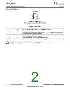
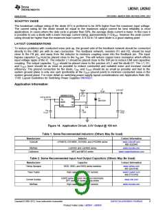
Connection Diagram
Top View
LM2840/1/2
CB
1
6
5
4
SW
GND
FB
2
3
V
IN
PIN 1 ID
SHDN
Figure 1. SOT 6 Lead
See Package Number DDC (R-PDSO-G6)
PIN DESCRIPTIONS
Pin
1
Name
CB
Function
SW FET gate bias voltage. Connect CBOOT cap between CB and SW.
Ground connection.
2
GND
Feedback pin: Set feedback voltage divider ratio with VOUT = VFB (1+(R1/R2)). Resistors should be
in the 100-10K range to avoid input bias errors.
3
4
FB
SHDN
Logic level shutdown input. Pull to GND to disable the device and pull high to enable the device. If
this function is not used tie to VIN or leave open.
5
6
VIN
Power input voltage pin: 4.5V to 42V normal operating range.
Power FET output: Connect to inductor, diode, and CBOOT cap.
SW
These devices have limited built-in ESD protection. The leads should be shorted together or the device placed in conductive foam
during storage or handling to prevent electrostatic damage to the MOS gates.
2
Submit Documentation Feedback
Copyright © 2009–2013, Texas Instruments Incorporated
Product Folder Links: LM2841 LM2842

 TI [ TEXAS INSTRUMENTS ]