LM2841, LM2842
www.ti.com
SNVS540H –MARCH 2009–REVISED APRIL 2013
SCHOTTKY DIODE
The breakdown voltage rating of the diode (D1) is preferred to be 25% higher than the maximum input voltage.
The current rating for the diode should be equal to the maximum output current for best reliability in most
applications. In cases where the duty cycle is greater than 50%, the average diode current is lower. In this case it
is possible to use a diode with a lower average current rating, approximately (1-D)IOUT, however the peak current
rating should be higher than the maximum load current. A 0.5A to 1A rated diode is a good starting point.
LAYOUT CONSIDERATIONS
To reduce problems with conducted noise pick up, the ground side of the feedback network should be connected
directly to the GND pin with its own connection. The feedback network, resistors R1 and R2, should be kept
close to the FB pin, and away from the inductor to minimize coupling noise into the feedback pin. The input
bypass capacitor CIN must be placed close to the VIN pin. This will reduce copper trace resistance which effects
input voltage ripple of the IC. The inductor L1 should be placed close to the SW pin to reduce EMI and capacitive
coupling. The output capacitor, COUT should be placed close to the junction of L1 and the diode D1. The L1, D1,
and COUT trace should be as short as possible to reduce conducted and radiated noise and increase overall
efficiency. The ground connection for the diode, CIN, and COUT should be as small as possible and tied to the
system ground plane in only one spot (preferably at the COUT ground point) to minimize conducted noise in the
system ground plane. For more detail on switching power supply layout considerations see Application Note AN-
1149: Layout Guidelines for Switching Power Supplies SNVA021.
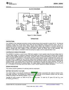
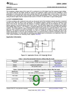
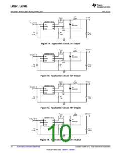
Application Information
L1
15 mH
3.3V OUT
C
BOOT
LM2840/1/2-ADJL
0.1 mF
4.5V to 42V IN
D1
MA2YD26
CB
V
IN
SHDN
GND
SW
FB
R1
3.4k
R2
1.02k
C
C
OUT
10 mF
IN
2.2 mF
Figure 14. Application Circuit, 3.3V Output @ 100 mA
Table 1. Some Recommended Inductors (Others May Be Used)
Manufacturer
Inductor
Contact Information
Coilcraft
LPS4018, DO1608C, DO3308, and LPO2506 series
www.coilcraft.com
800-3222645
MuRata
LQH55D and LQH66S series
MP2 and MP2A series
www.murata.com
Coiltronics
www.cooperbussman.com
Table 2. Some Recommended Input And Output Capacitors (Others May Be Used)
Manufacturer
Capacitor
Contact Information
Vishay Sprague
293D, 592D, and 595D series tantalum
www.vishay.com
407-324-4140
Taiyo Yuden
High capacitance MLCC ceramic
www.t-yuden.com
408-573-4150
ESRD seriec Polymer Aluminum Electrolytic
SPV and AFK series V-chip series
Cornell Dubilier
MuRata
www.cde.com
High capacitance MLCC ceramic
www.murata.com
Copyright © 2009–2013, Texas Instruments Incorporated
Submit Documentation Feedback
9
Product Folder Links: LM2841 LM2842

 TI [ TEXAS INSTRUMENTS ]