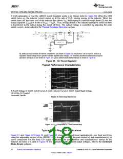
LM2587
SNVS115D –APRIL 2000–REVISED APRIL 2013
www.ti.com
The other method to reduce or eliminate the “ringing” is to insert a Schottky diode clamp between pins 4 and 3
(ground), also shown in Figure 56. This prevents the voltage at pin 4 from dropping below −0.4V. The reverse
voltage rating of the diode must be greater than the switch off voltage.
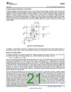
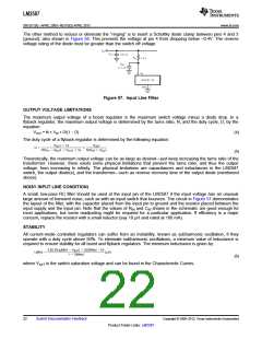
Figure 57. Input Line Filter
OUTPUT VOLTAGE LIMITATIONS
The maximum output voltage of a boost regulator is the maximum switch voltage minus a diode drop. In a
flyback regulator, the maximum output voltage is determined by the turns ratio, N, and the duty cycle, D, by the
equation:
VOUT ≈ N × VIN × D/(1 − D)
(4)
The duty cycle of a flyback regulator is determined by the following equation:
(5)
Theoretically, the maximum output voltage can be as large as desired—just keep increasing the turns ratio of the
transformer. However, there exists some physical limitations that prevent the turns ratio, and thus the output
voltage, from increasing to infinity. The physical limitations are capacitances and inductances in the LM2587
switch, the output diode(s), and the transformer—such as reverse recovery time of the output diode (mentioned
above).
NOISY INPUT LINE CONDITION)
A small, low-pass RC filter should be used at the input pin of the LM2587 if the input voltage has an unusual
large amount of transient noise, such as with an input switch that bounces. The circuit in Figure 57 demonstrates
the layout of the filter, with the capacitor placed from the input pin to ground and the resistor placed between the
input supply and the input pin. Note that the values of RIN and CIN shown in the schematic are good enough for
most applications, but some readjusting might be required for a particular application. If efficiency is a major
concern, replace the resistor with a small inductor (say 10 μH and rated at 100 mA).
STABILITY
All current-mode controlled regulators can suffer from an instability, known as subharmonic oscillation, if they
operate with a duty cycle above 50%. To eliminate subharmonic oscillations, a minimum value of inductance is
required to ensure stability for all boost and flyback regulators. The minimum inductance is given by:
(6)
where VSAT is the switch saturation voltage and can be found in the Characteristic Curves.
22
Submit Documentation Feedback
Copyright © 2000–2013, Texas Instruments Incorporated
Product Folder Links: LM2587

 TI [ TEXAS INSTRUMENTS ]