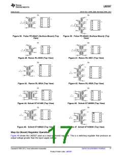
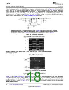
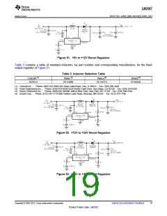
LM2587
www.ti.com
SNVS115D –APRIL 2000–REVISED APRIL 2013
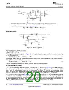
FLYBACK REGULATOR INPUT CAPACITORS
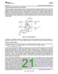
A flyback regulator draws discontinuous pulses of current from the input supply. Therefore, there are two input
capacitors needed in a flyback regulator; one for energy storage and one for filtering (see Figure 56). Both are
required due to the inherent operation of a flyback regulator. To keep a stable or constant voltage supply to the
LM2587, a storage capacitor (≥100 μF) is required. If the input source is a recitified DC supply and/or the
application has a wide temperature range, the required rms current rating of the capacitor might be very large.
This means a larger value of capacitance or a higher voltage rating will be needed of the input capacitor. The
storage capacitor will also attenuate noise which may interfere with other circuits connected to the same input
supply voltage.
Figure 56. Flyback Regulator
In addition, a small bypass capacitor is required due to the noise generated by the input current pulses. To
eliminate the noise, insert a 1.0 μF ceramic capacitor between VIN and ground as close as possible to the device.
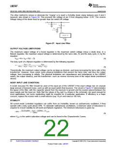
SWITCH VOLTAGE LIMITS
In a flyback regulator, the maximum steady-state voltage appearing at the switch, when it is off, is set by the
transformer turns ratio, N, the output voltage, VOUT, and the maximum input voltage, VIN (Max):
VSW(OFF) = VIN (Max) + (VOUT +VF)/N
(3)
where VF is the forward biased voltage of the output diode, and is 0.5V for Schottky diodes and 0.8V for ultra-fast
recovery diodes (typically). In certain circuits, there exists a voltage spike, VLL, superimposed on top of the
steady-state voltage (see Figure 22, waveform A). Usually, this voltage spike is caused by the transformer
leakage inductance and/or the output rectifier recovery time. To “clamp” the voltage at the switch from exceeding
its maximum value, a transient suppressor in series with a diode is inserted across the transformer primary (as
shown in the circuit on the front page and other flyback regulator circuits throughout the datasheet). The
schematic in Figure 56 shows another method of clamping the switch voltage. A single voltage transient
suppressor (the SA51A) is inserted at the switch pin. This method clamps the total voltage across the switch, not
just the voltage across the primary.
If poor circuit layout techniques are used (see the CIRCUIT LAYOUT GUIDELINES section), negative voltage
transients may appear on the Switch pin (pin 4). Applying a negative voltage (with respect to the IC's ground) to
any monolithic IC pin causes erratic and unpredictable operation of that IC. This holds true for the LM2587 IC as
well. When used in a flyback regulator, the voltage at the Switch pin (pin 4) can go negative when the switch
turns on. The “ringing” voltage at the switch pin is caused by the output diode capacitance and the transformer
leakage inductance forming a resonant circuit at the secondary(ies). The resonant circuit generates the “ringing”
voltage, which gets reflected back through the transformer to the switch pin. There are two common methods to
avoid this problem. One is to add an RC snubber around the output rectifier(s), as in Figure 56. The values of the
resistor and the capacitor must be chosen so that the voltage at the Switch pin does not drop below −0.4V. The
resistor may range in value between 10Ω and 1 kΩ, and the capacitor will vary from 0.001 μF to 0.1 μF. Adding a
snubber will (slightly) reduce the efficiency of the overall circuit.
Copyright © 2000–2013, Texas Instruments Incorporated
Submit Documentation Feedback
21
Product Folder Links: LM2587

 TI [ TEXAS INSTRUMENTS ]