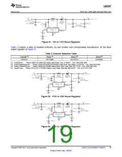
LM2587
www.ti.com
SNVS115D –APRIL 2000–REVISED APRIL 2013
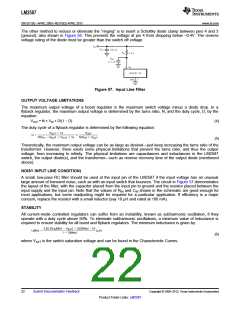
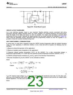
Figure 58. Circuit Board Layout
CIRCUIT LAYOUT GUIDELINES
As in any switching regulator, layout is very important. Rapidly switching currents associated with wiring
inductance generate voltage transients which can cause problems. For minimal inductance and ground loops,
keep the length of the leads and traces as short as possible. Use single point grounding or ground plane
construction for best results. Separate the signal grounds from the power grounds (as indicated in Figure 58).
When using the Adjustable version, physically locate the programming resistors as near the regulator IC as
possible, to keep the sensitive feedback wiring short.
HEAT SINK/THERMAL CONSIDERATIONS
In many cases, no heat sink is required to keep the LM2587 junction temperature within the allowed operating
range. For each application, to determine whether or not a heat sink will be required, the following must be
identified:
1) Maximum ambient temperature (in the application).
2) Maximum regulator power dissipation (in the application).
3) Maximum allowed junction temperature (125°C for the LM2587). For a safe, conservative design, a
temperature approximately 15°C cooler than the maximum junction temperature should be selected (110°C).
4) LM2587 package thermal resistances θJA and θJC (given in the Electrical Characteristics).
Total power dissipated (PD) by the LM2587 can be estimated as follows:
Boost:
(7)
VIN is the minimum input voltage, VOUT is the output voltage, N is the transformer turns ratio, D is the duty cycle,
and ILOAD is the maximum load current (and ∑ILOAD is the sum of the maximum load currents for multiple-output
flyback regulators). The duty cycle is given by:
Boost:
Copyright © 2000–2013, Texas Instruments Incorporated
Submit Documentation Feedback
23
Product Folder Links: LM2587

 TI [ TEXAS INSTRUMENTS ]