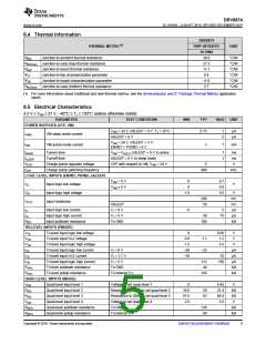
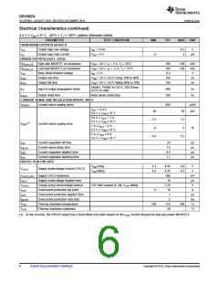
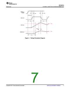
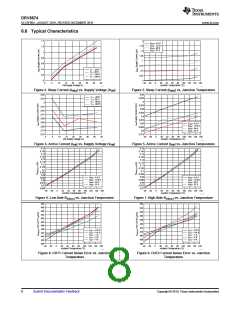
DRV8874
www.ti.com
SLVSF66A –AUGUST 2019–REVISED DECEMBER 2019
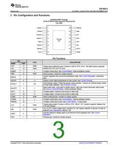
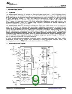
5 Pin Configuration and Functions
DRV8874 PWP Package
16-Pin HTSSOP With Exposed Thermal Pad
Top View
EN/IN1
PH/IN2
nSLEEP
nFAULT
VREF
1
2
3
4
5
6
7
8
16
15
14
13
12
11
10
9
PMODE
GND
CPL
CPH
Thermal
Pad
VCP
IPROPI
IMODE
OUT1
VM
OUT2
PGND
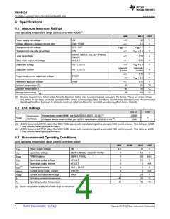
Pin Functions
PIN
TYPE
DESCRIPTION
NAME
CPH
PWP
13
PWR
PWR
I
Charge pump switching node. Connect a X5R or X7R, 22-nF, VM-rated ceramic capacitor
between the CPH and CPL pins.
CPL
14
EN/IN1
GND
1
H-bridge control input. See Control Modes. Internal pulldown resistor.
Device ground. Connect to system ground.
15
PWR
Current regulation and overcurrent protection mode. See Current Regulation. Quad-level
input.
IMODE
IPROPI
nFAULT
7
6
4
I
O
Analog current output proportional to load current. See Current Sensing.
Fault indicator output. Pulled low during a fault condition. Connect an external pullup resistor
for open-drain operation. See Protection Circuits.
OD
Sleep mode input. Logic high to enable device. Logic low to enter low-power sleep mode.
See Device Functional Modes. Internal pulldown resistor.
nSLEEP
3
I
OUT1
8
10
9
O
H-bridge output. Connect to the motor or other load.
OUT2
O
H-bridge output. Connect to the motor or other load.
PGND
PH/IN2
PMODE
PWR
Device power ground. Connect to system ground.
2
I
I
H-bridge control input. See Control Modes. Internal pulldown resistor.
H-bridge control input mode. See Control Modes. Tri-level input.
16
Charge pump output. Connect a X5R or X7R, 100-nF, 16-V ceramic capacitor between the
VCP and VM pins.
VCP
VM
12
11
PWR
PWR
4.5-V to 37-V power supply input. Connect a 0.1-µF bypass capacitor to ground, as well as
sufficient Bulk Capacitance rated for VM.
External reference voltage input to set internal current regulation limit. See Current
Regulation.
VREF
PAD
5
I
—
—
Thermal pad. Connect to system ground.
Copyright © 2019, Texas Instruments Incorporated
Submit Documentation Feedback
3

 TI [ TEXAS INSTRUMENTS ]