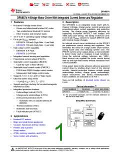
DRV8874
SLVSF66A –AUGUST 2019–REVISED DECEMBER 2019
www.ti.com
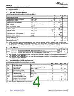
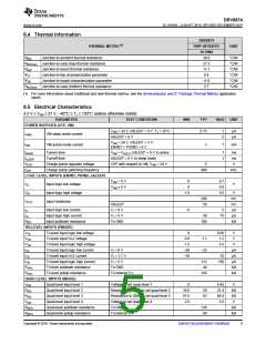
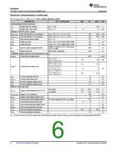
6 Specifications
6.1 Absolute Maximum Ratings
over operating temperature range (unless otherwise noted)(1)
MIN
–0.3
MAX
40
UNIT
Power supply pin voltage
VM
V
V
V
V
Voltage difference between ground pins
Charge pump pin voltage
GND, PGND
CPH, VCP
CPL
–0.3
0.3
VVM – 0.3
–0.3
VVM + 7
VVM + 0.3
Charge pump low-side pin voltage
EN/IN1, IMODE, nSLEEP, PH/IN2,
PMODE
Logic pin voltage
–0.3
5.75
V
Open-drain output pin voltage
Output pin voltage
nFAULT
–0.3
–0.9
5.75
V
V
OUT1, OUT2
VVM + 0.9
Internally
Limited
Internally
Limited
Output pin current
OUT1, OUT2
A
–0.3
–0.3
–0.3
–40
–40
–65
5.75
VVM + 0.3
5.75
V
V
Proportional current output pin voltage
IPROPI
VREF
Reference input pin voltage
Ambient temperature, TA
Junction temperature, TJ
Storage temperature, Tstg
V
125
°C
°C
°C
150
150
(1) Stresses beyond those listed under Absolute Maximum Rating may cause permanent damage to the device. These are stress ratings
only, which do not imply functional operation of the device at these or any other conditions beyond those indicated under Recommended
Operating Condition. Exposure to absolute-maximum-rated conditions for extended periods may affect device reliability.
6.2 ESD Ratings
VALUE
±2000
±500
UNIT
Human body model (HBM), per ANSI/ESDA/JEDEC JS-001(1)
Charged device model (CDM), per JEDEC specification JESD22-C101(2)
Electrostatic
discharge
V(ESD)
V
(1) JEDEC document JEP155 states that 500-V HBM allows safe manufacturing with a standard ESD control process. Pins listed as ± 2000
V may actually have higher performance.
(2) JEDEC document JEP157 states that 250-V CDM allows safe manufacturing with a standard ESD control process. Pins listed as ± 500
V may actually have higher performance.
6.3 Recommended Operating Conditions
over operating temperature range (unless otherwise noted)
MIN
4.5
0
NOM
MAX
37
UNIT
V
VVM
VIN
Power supply voltage
VM
Logic input voltage
EN/IN1, MODE, nSLEEP, PH/IN2
5.5
100
5.5
5
V
fPWM
VOD
IOD
PWM frequency
EN/IN1, PH/IN2
nFAULT
0
kHz
V
Open drain pullup voltage
Open drain output current
Peak output current
0
nFAULT
0
mA
A
(1)
IOUT
IIPROPI
VVREF
TA
OUT1, OUT2
IPROPI
0
6
Current sense output current
Current limit reference voltage
Operating ambient temperature
Operating junction temperature
0
3
mA
V
VREF
0
3.6
125
150
–40
–40
°C
°C
TJ
(1) Power dissipation and thermal limits must be observed
4
Submit Documentation Feedback
Copyright © 2019, Texas Instruments Incorporated

 TI [ TEXAS INSTRUMENTS ]