DRV8874
SLVSF66A –AUGUST 2019–REVISED DECEMBER 2019
www.ti.com
8.2.2.1 Design Requirements
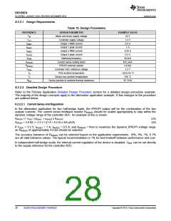
Table 10. Design Parameters
REFERENCE
VM
DESIGN PARAMETER
Motor and driver supply voltage
EXAMPLE VALUE
24 V
VCC
Controller supply voltage
Output 1 RMS current
3.3 V
IRMS1
IPEAK1
IRMS2
IPEAK2
fPWM
0.5 A
Output 1 peak current
1 A
Output 2 RMS current
0.25 A
Output 2 peak current
0.5 A
Switching frequency
20 kHz
455 µA/A
4.8 kΩ
AIPROPI
RIPROPI
VADC
TA
Current sense scaling factor
IPROPI external resistor
Controller ADC reference voltage
PCB ambient temperature
Device max junction temperature
Device junction to ambient thermal resistance
3.3 V
–20 to 85 °C
150 °C
35 °C/W
TJ
RθJA
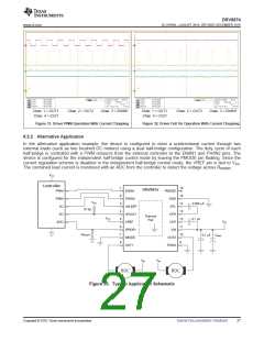
8.2.2.2 Detailed Design Procedure
Refer to the Primary Application Detailed Design Procedure section for a detailed design procedure example.
The majority of the design concepts apply to the alternative application example. A few changes to the procedure
are outlined below.
8.2.2.2.1 Current Sense and Regulation
In the alternative application for two half-bridge loads, the IPROPI output will be the combination of the two
outputs currents. The current sense feedback resistor RIPROPI should be scaled appropriately to stay within the
dynamic voltage range of the controller ADC. An example of this is shown
RIPROPI <= VADC / ((IPEAK1 + IPEAK2) x AIPROPI
)
(23)
(24)
RIPROPI = 4.8 kΩ <= 3.3 V / ((1 A + 0.5 A) x 455 µA/A)
If VADC = 3.3 V, IPEAK1 = 1 A, IPEAK2 = 0.5 A, and AIPROPI = then to maximize the dynamic IPROPI voltage range
an RIPROPI of approximately 4.8 kΩ should be selected.
The accuracy tolerance of RIPROPI can be selected based on the application requirements. 10%, 5%, 1%, 0.1%
are all valid tolerance values. The typical recommendation is 1% for best tradeoff between performance and cost.
In independent half-bridge mode, the internal current regulation of the device is disabled. VREF can be set directly
to the supply reference for the controller ADC.
28
Submit Documentation Feedback
Copyright © 2019, Texas Instruments Incorporated

 TI [ TEXAS INSTRUMENTS ]