DRV8874
www.ti.com
SLVSF66A –AUGUST 2019–REVISED DECEMBER 2019
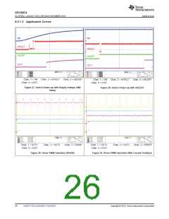
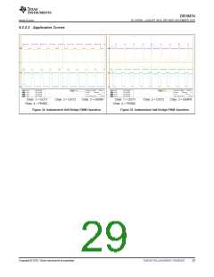
Chan. 1 = OUT1
Chan. 4 = IOUT
Chan. 2 = OUT2
Chan. 3 = EN/IN1
Chan. 1 = OUT1
Chan. 4 = IOUT
Chan. 2 = OUT2
Chan. 3 = EN/IN1
Figure 31. Driver PWM Operation With Current Chopping
Figure 32. Driver Full On Operation With Current Chopping
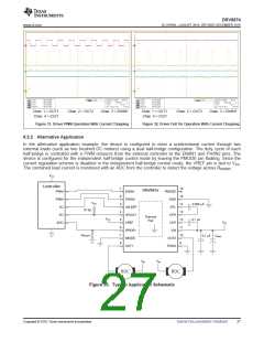
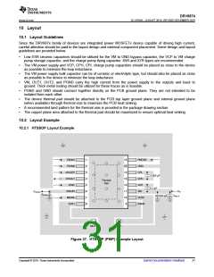
8.2.2 Alternative Application
In the alternative application example, the device is configured to drive a unidirectional current through two
external loads (such as two brushed DC motors) using a dual half-bridge configuration. The duty cycle of each
half-bridge is controlled with a PWM resource from the external controller to the EN/IN1 and PH/IN2 pins. The
device is configured for the independent half-bridge control mode by leaving the PMODE pin floating. Since the
current regulation scheme is disabled in the independent half-bridge control mode, the VREF pin is tied to VCC
.
The combined load current is monitored with an ADC from the controller to detect the voltage across RIPROPI
.
VCC
Controller
1
2
3
4
5
6
7
8
16
X
DRV887x
PWM
PWM
I/O
EN/IN1
PH/IN2
nSLEEP
nFAULT
VREF
PMODE
GND
CPL
15
14
13
12
11
10
9
VCC
0.022 …F
0.1 …F
10 kꢀ
I/O
CPH
Thermal
Pad
VCC
VM
ADC
VCP
IPROPI
IMODE
OUT1
VM
RIPROPI
0.1 …F CBulk
OUT2
PGND
VM
VM
BDC
BDC
Figure 33. Typical Application Schematic
Copyright © 2019, Texas Instruments Incorporated
Submit Documentation Feedback
27

 TI [ TEXAS INSTRUMENTS ]