DRV8874
www.ti.com
SLVSF66A –AUGUST 2019–REVISED DECEMBER 2019
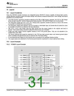
10 Layout
10.1 Layout Guidelines
Since the DRV887x family of devices are integrated power MOSFETs device capable of driving high current,
careful attention should be paid to the layout design and external component placement. Some design and layout
guidelines are provided below.
•
•
•
•
•
•
Low ESR ceramic capacitors should be utilized for the VM to GND bypass capacitor, the VCP to VM charge
pump storage capacitor, and the charge pump flying capacitor. X5R and X7R types are recommended.
The VM power supply and VCP, CPH, CPL charge pump capacitors should be placed as close to the device
as possible to minimize the loop inductance.
The VM power supply bulk capacitor can be of ceramic or electrolytic type, but should also be placed as close
as possible to the device to minimize the loop inductance.
VM, OUT1, OUT2, and PGND carry the high current from the power supply to the outputs and back to
ground. Thick metal routing should be utilized for these traces as is feasible.
PGND and GND should connect together directly on the PCB ground plane. They are not intended to be
isolated from each other.
The device thermal pad should be attached to the PCB top layer ground plane and internal ground plane
(when available) through thermal vias to maximize the PCB heat sinking.
•
•
A recommended land pattern for the thermal vias is provided in the package drawing section.
The copper plane area attached to the thermal pad should be maximized to ensure optimal heat sinking.
10.2 Layout Example
10.2.1 HTSSOP Layout Example
EN/IN1
PH/IN2
nSLEEP
nFAULT
VREF
1
2
3
4
5
6
7
8
16
15
14
13
12
11
10
9
PMODE
GND
CPL
0.022 …F
0.1 …F
CPH
Thermal
Pad
VCP
IPROPI
IMODE
OUT1
VM
VM
CBULK
VIPROPI
RIPROPI
0.1 …F
OUT2
PGND
MOT+
MOT-
Figure 37. HTSSOP (PWP) Example Layout
Copyright © 2019, Texas Instruments Incorporated
Submit Documentation Feedback
31

 TI [ TEXAS INSTRUMENTS ]