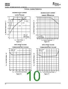
DRV593
DRV594
www.ti.com
SLOS401A - SEPTEMBER 2002 REVISED - OCTOBER 2002
V
DD
1 µF
10 µF
10 µH
1 µF
To TEC or Laser
Diode Anode
AVDD
PWM
PGND
PGND
PGND
PGND
PGND
PGND
H/C
AGND (Connect to PowerPAD)
120 kΩ
ROSC
COSC
220 pF
DC Control
Voltage
DRV593
DRV594
AREF
1 µF
IN+
1 kΩ
1 kΩ
10 µF
IN-
SHUTDOWN
Shutdown Control
FAULT1
FAULT0
To TEC or Laser
Diode Cathode
1 µF
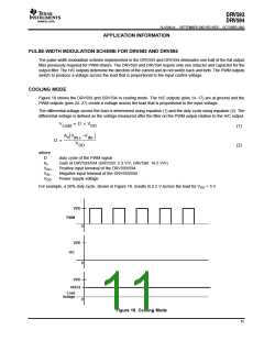
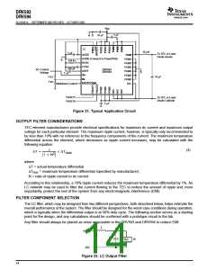
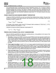
Figure 21. Typical Application Circuit
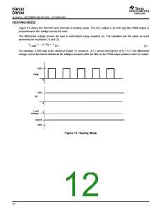
OUTPUT FILTER CONSIDERATIONS
TEC element manufacturers provide electrical specifications for maximum dc current and maximum output
voltage for each particular element. The maximum ripple current, however, is typically only recommended to
be less than 10% with no reference to the frequency components of the current. The maximum temperature
differential across the element, which decreases as ripple current increases, may be calculated with the
following equation:
(4)
1
DT +
DT
max
2
ǒ
Ǔ
1 ) N
where
∆T = actual temperature differential
∆T = maximum temperature differential (specified by manufacturer)
max
N = ratio of ripple current to dc current
According to this relationship, a 10% ripple current reduces the maximum temperature differential by 1%. An
LC network may be used to filter the current flowing to the TEC to reduce the amount of ripple and, more
importantly, protect the rest of the system from any electromagnetic interference (EMI).
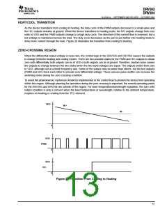
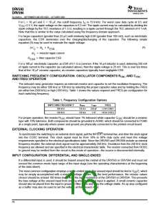
FILTER COMPONENT SELECTION
The LC filter, which may be designed from two different perspectives, both described below, helps estimate the
overall performance of the system. The filter should be designed for the worst-case conditions during operation,
which is typically when the differential output is at 50% duty cycle. The following section serves as a starting
point for the design, and any calculations should be confirmed with a prototype circuit in the lab.
Any filter should always be placed as close as possible to the DRV593 and DRV594 to reduce EMI.
L
PWM
C
R
TEC
H/C
Figure 22. LC Output Filter
14

 TI [ TEXAS INSTRUMENTS ]