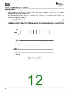
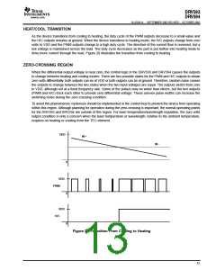
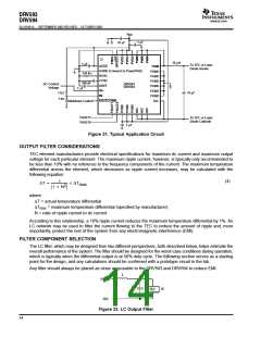
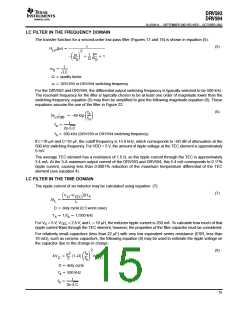
DRV593
DRV594
www.ti.com
SLOS401A - SEPTEMBER 2002 REVISED - OCTOBER 2002
For L = 10 µH and C = 10 µF, the cutoff frequency, f , is 15.9 kHz. For worst case duty cycle of 0.5 and
o
V
=2.5 V, the ripple voltage on the capacitors is 6.2 mV. The ripple current may be calculated by dividing the
TEC
ripple voltage by the TEC resistance of 1.5 Ω, resulting in a ripple current through the TEC element of 4.1 mA.
Note that this is similar to the value calculated using the frequency domain approach.
For larger capacitors (greater than 22 µF) with relatively high ESR (greater than 100 mΩ), such as electrolytic
capacitors, the ESR dominates over the charging/discharging of the capacitor. The following simple
equation (9) may be used to estimate the ripple voltage:
(9)
DV + DI R
L
C
ESR
DI + inductor ripple current
L
R
+ filter capacitor ESR
ESR
For a 100 µF electrolytic capacitor, an ESR of 0.1 Ω is common. If the 10 µH inductor is used, delivering 250 mA
of ripple current to the capacitor (as calculated above), then the ripple voltage is 25 mV. This is over ten times
that of the 10 µF ceramic capacitor, as ceramic capacitors typically have negligible ESR.
SWITCHING FREQUENCY CONFIGURATION: OSCILLATOR COMPONENTS ROSC AND COSC
AND FREQ OPERATION
The onboard ramp generator requires an external resistor and capacitor to set the oscillation frequency. The
frequency may be either 500 kHz or 100 kHz by selecting the proper capacitor value and by holding the FREQ
pin either low (500 kHz) or high (100 kHz). Table 1 shows the values required and FREQ pin configuration for
each switching frequency.
Table 1. Frequency Configuration Options
SWITCHING FREQUENCY
500 kHz
R
C
FREQ
OSC
OSC
120 kΩ
120 kΩ
220 pF
1 nF
LOW (GND)
HIGH (VDD)
100 kHz
For proper operation, the resistor R
should have 1% tolerance while capacitor C
should be a ceramic
OSC
OSC
type with 10% tolerance. Both components should be grounded to AGND, which should be connected to PGND
at a single point, typically where power and ground are physically connected to the printed-circuit board.
EXTERNAL CLOCKING OPERATION
To synchronize the switching to an external clock signal, pull the INT/EXT terminal low, and drive the clock signal
into the COSC terminal. This clock signal must be from 10% to 90% duty cycle and meet the voltage
requirements specified in the electrical specifications table. Since the DRV593 and DRV594 include an internal
frequency doubler, the external clock signal must be approximately 250 kHz. Deviations from the 250 kHz clock
frequency are allowed and are specified in the electrical characteristic table. The resistor connected from ROSC
to ground may be omitted from the circuit in this mode of operation—the source is disconnected internally.
INPUT CONFIGURATION: DIFFERENTIAL AND SINGLE-ENDED
If a differential input is used, it should be biased around the midrail of the DRV593 or DRV594 and must not
exceed the common-mode input range of the input stage (see the operating characteristics at the beginning
of the data sheet).
The most common configuration employs a single-ended input. The unused input should be tied to V /2, which
DD
may be simply accomplished with a resistive voltage divider. For the best performance, the resistor values
chosen should be at least 100 times lower than the input resistance of the DRV593 or DRV594. This prevents
the bias voltage at the unused input from shifting when the signal input is applied. A small ceramic capacitor
should also be placed from the input to ground to filter noise and keep the voltage stable. An op amp configured
as a buffer may also be used to set the voltage at the unused input.
16

 TI [ TEXAS INSTRUMENTS ]