DRV593
DRV594
www.ti.com
SLOS401A - SEPTEMBER 2002 REVISED - OCTOBER 2002
The overtemperature fault is reported when the junction temperature exceeds 115°C. The device continues
operating normally until the junction temperature reaches 150°C, at which point the IC is disabled to prevent
permanent damage from occurring. The system’s controller must reduce the power demanded from the
DRV593 or DRV594 once the overtemperature flag is set, or else the device switches off when it reaches 150°C.
This fault is not latched; once the junction temperature drops below 115°C, the fault is cleared, and normal
operation resumes.
POWER DISSIPATION AND MAXIMUM AMBIENT TEMPERATURE
Though the DRV593 and DRV594 are much more efficient than traditional linear solutions, the power drop
across the on-resistance of the output transistors does generate some heat in the package, which may be
calculated as shown in equation (11):
+ ǒIOUTǓ2
(11)
P
r
DISS
DS(on), total
For example, at the maximum output current of 3 A through a total on-resistance of 130 mΩ (at T = 25°C),
J
the power dissipated in the package is 1.17 W.
Calculate the maximum ambient temperature using equation (12):
(12)
* ǒθ
JA
DISSǓ
T
+ T
P
A
J
PRINTED-CIRCUIT BOARD (PCB) LAYOUT CONSIDERATIONS
Since the DRV593 and DRV594 are high-current switching devices, a few guidelines for the layout of the
printed-circuit board (PCB) must be considered:
1. Grounding. Analog ground (AGND) and power ground (PGND) must be kept separated, ideally back to
where the power supply physically connects to the PCB, minimally back to the bulk decoupling capacitor
(10 µF ceramic minimum). Furthermore, the PowerPAD ground connection should be made to AGND, not
PGND. Ground planes are not recommended for AGND or PGND, traces should be used to route the
currents. Wide traces (100 mils) should be used for PGND while narrow traces (15 mils) should be used
for AGND.
2. Power supply decoupling. A small 0.1 µF to 1 µF ceramic capacitor should be placed as close to each
set of PVDD pins as possible, connecting from PVDD to PGND. A 0.1 µF to 1 µF ceramic capacitor should
also be placed close to the AVDD pin, connecting from AVDD to AGND. A bulk decoupling capacitor of at
least 10 µF, preferably ceramic, should be placed close to the DRV593 or DRV594, from PVDD to PGND.
If power supply lines are long, additional decoupling may be required.
3. Power and output traces. The power and output traces should be sized to handle the desired maximum
output current. The output traces should be kept as short as possible to reduce EMI, i.e., the output filter
should be placed as close to the DRV593 or DRV594 outputs as possible.
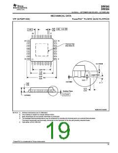
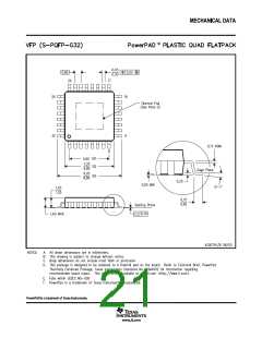
4. PowerPAD. The DRV593 and DRV594 in the Quad Flatpack package use TI’s PowerPAD technology to
enhance the thermal performance. The PowerPAD is physically connected to the substrate of the DRV593
and DRV594 silicon, which is connected to AGND. The PowerPAD ground connection should therefore be
kept separate from PGND as described above. The pad underneath the AGND pin may be connected
underneath the device to the PowerPAD ground connection for ease of routing. For additional information
on PowerPAD PCB layout, refer to the PowerPAD Thermally Enhanced Package application note,
SLMA002.
5. Thermal performance. For proper thermal performance, the PowerPAD must be soldered down to a
thermal land, as described in the PowerPAD Thermally Enhanced Package application note, SLMA002.
In addition, at high current levels (greater than 2 A) or high ambient temperatures (greater than 25°C), an
internal plane may be used for heat sinking. The vias under the PowerPAD should make a solid connection,
and the plane should not be tied to ground except through the PowerPAD connection, as described above.
18

 TI [ TEXAS INSTRUMENTS ]