DRV593
DRV594
www.ti.com
SLOS401A - SEPTEMBER 2002 REVISED - OCTOBER 2002
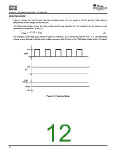
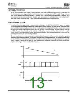
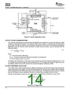
APPLICATION INFORMATION
PULSE-WIDTH MODULATION SCHEME FOR DRV593 AND DRV594
The pulse-width modulation scheme implemented in the DRV593 and DRV594 eliminates one-half of the full output
filter previously required for PWM drivers. The DRV593 and DRV594 require only one inductor and capacitor for the
output filter. The H/C outputs determine the direction of the current and do not switch back and forth. The PWM outputs
switch to produce a voltage across the load that is proportional to the input control voltage.
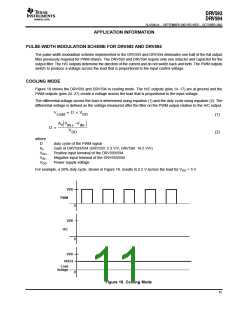
COOLING MODE
Figure 18 shows the DRV593 and DRV594 in cooling mode. The H/C outputs (pins 14-17) are at ground and the
PWM outputs (pins 24-27) create a voltage across the load that is proportional to the input voltage.
The differential voltage across the load is determined using equation (1) and the duty cycle using equation (2). The
differential voltage is defined as the voltage measured after the filter on the PWM output relative to the H/C output.
V
+ D V
Load
DD
(1)
vǒV
IN–Ǔ
A
–V
IN)
V
D +
DD
(2)
where
D
duty cycle of the PWM signal
Av
Gain of DRV593/594 (DRV593: 2.3 V/V, DRV594: 14.5 V/V)
Positive input terminal of the DRV593/594
Negative input terminal of the DRV593/594
Power supply voltage
VIN+
VIN-
VDD
For example, a 50% duty cycle, shown in Figure 18, results in 2.5 V across the load for VDD = 5 V.
VDD
PWM
0
VDD
H/C
0
VDD
VDD/2
Load
Voltage
0
Figure 18. Cooling Mode
11

 TI [ TEXAS INSTRUMENTS ]