5.0 DP83840A Application
By placing chassis ground on the top and bottom layers,
additional EMI shielding is created around the 125 Mb/s
signal traces that must be routed between the magnetics and
the RJ45-8 media connector. The example in Figure 17
assumes the use of Micro-Strip impedance control
techniques for trace routing.
5.1 Typical Board Level Application
Figure 20 shows a typical implementation of a 10/100
Mb/s Ethernet node application. This is given only to
indicate the major circuit elements of such a design. It is
not intended to be a full circuit diagram. For detailed
system level application information please contact your
National Semiconductor sales representative.
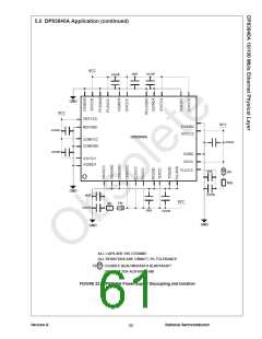
5.3 POWER AND GROUND FILTERING
Sufficient filtering between the DP83840A power and ground
pins placed as near to these pins as possible is
recommended. Figure 22 suggests one option for device
noise filtering including special consideration for the sensitive
analog and PLL power pins. The actual connection from
ANAVCC to the 4Ω resistor should be implemented as a ‘fat
etch’ (20 to 30 mils wide) of minimum length. The same
technique should be implemented for the connection from
PLLVCC to its 10Ω resistor.
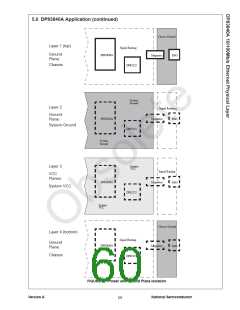
5.2 PLANE PARTITIONING
The recommendations for power plane partitioning
provided herein represent a more simplified approach
when compared to earlier recommendations. By
reducing the number of instances of plane partitioning
within a given system design, empirical data has shown
a
resultant improvement (reduction) in radiated
emissions testing. Additionally, be eliminating power
plane partitioning within the system Vcc and system
ground domains, specific impedance controlled signal
routing can remain uninterrupted.
The example provided in Figure 22 has been designed to
minimize the number of physical decoupling components
while still maintaining good overall device decoupling.
Figure 21 illustrates one possible example of plane
partitioning and allocation assuming a typical four-layer
board design. The minimum gap between any two
planes on a single layer must be held to 125 mils.
V
CC
TXU +/-
TXS +/-
TX_CLK
TXD<3:0>
TX_EN
26, 25
24, 23
75, 76, 77, 78
82
RXI+/-
74
21, 20
1
V
DP83840A
CC
TD+
CRS
COL
2
66
65
TD-
TD +/-
3
6
17, 16
15, 16
MEDIA
ACCESS
CONTROLLER
TXD +/-
RXD +/-
RD+
RD-
RXD<3:0>
RX_CLK
RX_DV
RX_ER
MDC
9, 8
2, 1
55, 56, 57, 58
RD +/-
SD +/-
62
64
63
72
67
5, 6
8, 7
54
25, 24
20, 21
RJ-45
SPEED_10
ENCSEL
LBEN
DP83223
TWISTER
53
12
MDIO
19
49
2
33
X1
4
OSCIN
GND
V
CC
GND
4.7k
50 MHz
0.005%
V
CC
GND
FIGURE 20. Typical 10/100 Ethernet Node Design Device Interconnection
Version A
58
National Semiconductor

 TI [ TEXAS INSTRUMENTS ]