6.0 Hardware User Information
a node application the Media Access Controller (MAC)
would need to decipher if the data that was being received
was bad.
6.1 Jabber/Timeout
Problem:
During the CRS_Jabber fix implemented on the
DP83840A, an unforeseen condition has resulted in
undesirable behavior in the CRS signal. There exists a
narrow region of improper CRS activity at the end of the
722µs timeout where the device recognizes the Jabber
function.
Solution/Workaround:
There is no current workaround to this problem. This
problem will be corrected in future products.
6.3 Link LED, Link Status Bit
Problem:
Description:
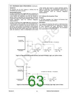
If the data packet is essentially the same length as the
default 722µs descrambler timeout CRS glitching will
occur. More specifically if the data packet terminates within
600ns of the 722µs descrambler timeout, then the
descrambler won’t have sufficient time to recognize the
necessary 15 idles before it times out. In that case the
parallel CRS_JAB (internal signal) will assert CRS to
indicate a jabber event.
The Link LED which indicates good link status derives its
signal from energy present on Signal Detect (SD+/-). The
Link Status bit (bit 2) in the Basic Mode Control Register
(00h) represents true link and derives its status from
different conditions than the Link LED.
Description:
The Basic Status Register Link status operation is as
follows:
Symptoms:
Since normal Ethernet packet activity is constrained to a
maximum packet size of 1514 bytes, which is about 121µs,
the CRS glitch will not show up with standard packet
lengths. In the case that packets fall within the narrow
range for CRS glitching, that packet will be lost. The next
packet could be lost if the Inner-Packet-Gap (IPG) is too
This bit represents true link. In 100Base-TX it is Cipher in
Sync. Cipher-in-sync is based on receiving 15 idle symbols
after Link Test Fail (LTF) is low.
If link status is down it is updated in the bit, next clock
cycle.
small relative to the CRS glitch, which varies from To get the link status, the user has to read the register
approximately 40ns to 600ns.
twice. The last read will give the correct status, after the
first read bit is updated with the new link status. This
register bit operation is based on IEEE 802.3u (page 31,
802.3u/D5.3).
Solution/Workaround:
There is no current workaround to this problem. This
problem will be corrected in the next silicon revision.
Symptoms:
It is possible for Link LED to have a different value than the
Link Status Register bit.
6.2 Link Timer
Problem:
Solution/Workaround:
For True Link, read the register status bit twice. The
operation of the Link is IEEE 802.3 compliant.
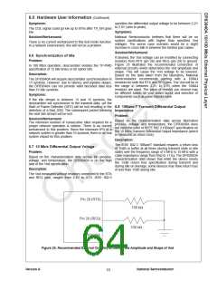
Link Timer State Machine Counter will not reset to 0 if the
Signal Detect falls while the Link Timer is in the
HYSTERESIS state.
Description:
6.4 PHYAD[3] and SPEED_100
Problem:
If the link state machine is in the HYSTERESIS state
(Figure 24-15, clause 24.3.4.4 of 802.3u/D5.3), the timer
counts down from 500 to 0. AT 0, link timer is done, the
state machine transitions, and the timer is reset to 500. If
Signal Detect falls while the link state machine is in the
HYSTERSIS state, the state machine goes back to
LINK_DOWN, but the timer does not reset, since the reset
condition is based on the timer reaching 0. Thus when
Signal Detect becomes asserted, the counter will resume
counting where it left off, and not count the full 500µs.
When using the SPEED_100 output (pin 89) of the
DP83840A to control external circuitry such as certain
switch elements for Common Magnetics implementations,
care must be taken in order to avoid electrical contention
between the effective load of the external circuitry and the
power-on/reset latch-in value of the PHYAD[3] input (also
pin 89).
Description:
Symptoms:
The standard procedure for latching in the desired PHY
Address of the DP83840A during power-on/reset is to
resistively tie each of the five PHYAD pins either high or
low such that one of the 32 possible addresses is
programmed into the device. If the dual purpose PHYAD
pin is connected to an external load which contends with
the intended pull-up or pull-down resistor, the wrong logic
level may be latched into the device which will result in an
invalid (unintended) PHY address. This, in turn, will impair
serial MII management of the PDP83840A.
If the network is operating normally and receiving good
data (Normal Link, substantial number of idles) no
problems will be observed. If Signal Detect is varying (bad
reception) the part would try to lock. If the lock was
successful the DP83840A would report Bad Start of
Stream Delimiter (Bad SSD) and the device would
disconnect. In a Repeater application the DP83840A would
see two Bad SSD’s and disconnect that port. Only one
packet would be lost and then the part would reconnect. In
Version A
National Semiconductor
61

 TI [ TEXAS INSTRUMENTS ]