6.0 Hardware User Information (Continued)
Symptoms:
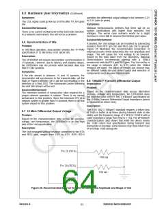
1.2kΩ resistor with respect to proper transistor biasing.
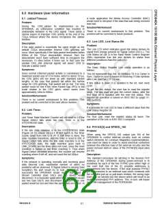
Figure 24 illustrates the recommended connection of
external circuitry when using PHYAD[3] / SPEED_100 to
control transistors used for Common Magnetics
implementations.
An improper five bit PHY Address is latched into the
DP83840A upon power-on/reset.
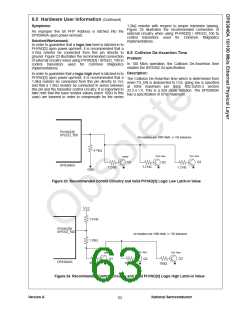
Solution/Workaround:
In order to guarantee that a logic low level is latched-in to
PHYAD[3] upon power-up/reset, it is recommended that a
4.7kΩ resistor be connected from this pin directly to
ground. Figure 23 illustrates the recommended connection
of external circuitry when using PHYAD[3] / SPEED_100 to
control transistors used for Common Magnetics
implementations.
6.5 Collision De-Assertion Time
Problem:
In 100 Mb/s operation, the Collision De-Assertion time
violates the IEEE802.3u specification.
Description:
In order to guarantee that a logic high level is latched-in to
PHYAD[3] upon power-up/reset, it is recommended that a
1.0kΩ resistor be connected from this pin directly to Vcc
and that a 1.2kΩ resistor be connected in series between
this pin and the transistor control circuitry. It is important to
take note that the base resistor values (each 100Ω in this
case) are lowered in order to compensate for the series
The Collision De-Assertion time which is determined from
when TX_EN is deasserted to COL going low is specified
at 40ns maximum per IEEE 802.3u/D5.3 section
22.2.4.1.9. This is a test mode function. The DP83840A
has a specification of 87ns maximum.
PHYAD[3]/
SPEED_100
All resistors are 1/8th Watt, +/- 5% tolerance
4.7kΩ
TXO+ Term
TXO- Term
TXREF
Q3
Q1
Q2
DP83840A
1.2 kΩ
1.2 kΩ
1.2 kΩ
GND
Figure 23. Recommended Control Circuitry and Valid PHYAD[3] Logic Low Latch-in Value
Vcc
1.0 kΩ
PHYAD[3]/
SPEED_100
All resistors are 1/8th Watt, +/- 5% tolerance
1.2kΩ
TXO+ Term
TXO- Term
TXREF
Q3
Q1
Q2
DP83840A
100Ω
100Ω
100Ω
Figure 24. Recommended Control Circuitry and Valid PHYAD[3] Logic High Latch-in Value
Version A
National Semiconductor
62

 TI [ TEXAS INSTRUMENTS ]