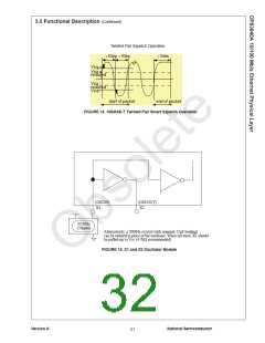
3.0 Functional Description (Continued)
product. The IEEE 1149.1 Boundary Scan Architecture are connected to system output pins. This ensures that
document should be referenced for additional detail.
known data is driven through the system output pins upon
entering the Extest instruction.
The circuitry defined by this standard allows test
instructions and associated data to be input serially into a Without Preload, indeterminate data would be driven until
device. The instruction execution results are output serially. the first scan sequence has been completed. The shifting
of data for the Sample and Preload phases can occur
The DP83840A reserves five pins, called the Test Access
simultaneously. While data capture is being shifted out, the
Port (TAP), to provide test access: TMS, TCK, Test Data
preload data can be shifted in.
Input (TDI), Test Data Output (TDO) and Test Reset
(TRST). These signals are described in Section 2.7. To 3.8.1.4 Extest Instruction
ensure race-free operation all input and output data is
The Extest instruction allows circuitry external to the
synchronous to the test clock (TCK). TAP input signals
DP83840A (typically the board interconnections) to be
(TMS and TDI) are clocked into the test logic on the rising
tested.
edge of TCK while output signal (TDO) is clocked on the
falling edge.
Prior to executing the Extest instruction, the first test
stimulus to be applied will be shifted into the boundary-
scan registers using the Sample/Preload instruction. Thus,
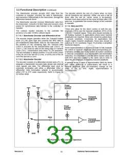
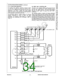
3.8.1 Test Logic
The IEEE 1149.1 Test Logic consists of a Test Access Port when the change to the Extest instruction takes place,
(TAP) controller, an instruction register, and a group of test known data will be driven immediately from the DP83840A
data registers including Bypass, Device Identification and to its external connections.
Boundary Scan registers.
This provides stimulus to the system input pins of adjacent
The TAP controller is a synchronous 16 state machine that devices on the assembled printed circuit boards. Figure 14
responds to changes at the TMS and TCK signals.
below illustrates the IEEE 1149.1 architecture.
This controls the sequence of operations by generating 3.8.2 Device Testing
clock and control signals to the instruction and test data
registers. The control signals switch TDI and TDO between
instruction and test data registers.
IEEE 1149.1 provides a simple solution for testing many of
the standard static pin parametrics. Reasonably accurate
limits may be tested as a functional pattern.
The DP83840A implements 4 basic instructions: ID_Code,
bypass, Sample/Preload and Extest. Upon reset, the
ID_Code instruction is selected by default. If the ID_Code
instruction is not supported, the bypass instruction is
selected instead.
The IEEE 1149.1 test circuitry is tested itself as a
consequence of testing pin parametrics. Specific tests are:
TRI-STATE conditions of TDO when serial shift
between TDI and TDO is not selected
3.8.1.1 ID_Code Instruction
Input leakage of TCK, TMS, TDI and TRST
Output has TRI-STATE leakage of TDO
The ID_Code instruction allows users to select the 32-bit
IDCODE register and interrogate the contents which
consist of the manufacturer's ID, part ID and the version
number.
Opens and shorts of TCK, TMS, TDI, TRST, and TDO
IDCODE register, the bypass register and the TAP
controller state machine sequences
3.8.1.2 Bypass Instruction
Open and shorted pins can be identified by placing an
alternating bit pattern
The bypass instruction uses the bypass register. The
bypass register contains a single shift-register stage and is
used to provide a minimum length serial path between the
TDI and TDO pins of the DP83840A when test operation is
not required. This allows more rapid movement of test data
to and from other testable devices in the system.
on the I/O pins. Any shorted bond wires would either cause
an input to be misinterpreted in the inputs scan phase, or
the test comparator would fail an output during data scan.
Repeating the test with the inverse bit pattern provides
coverage of VCC and GND short/open circuits.
3.8.1.3 Sample/Preload Instruction
The Sample/Preload instruction allows scanning of the
boundary-scan register without causing interference to the
normal operation of the on-chip system logic.
3.8.3 Boundary Scan Description Language File
A Boundary Scan Description Language (BSDL) file is
available. Contact your local National Semiconductor
representative to obtain the latest version.
Two functions are performed when this instruction is
selected.
Sample allows a snapshot to be taken of the data flowing
from the system pins to the on-chip test logic or vice versa,
without interfering with normal operation. The snapshot is
taken on the rising edge of TCK in the Capture-DR
controller state, and the data can be viewed by shifting
through the component's TDO output.
While sampling and shifting data out through TDO for
observation, preload allows an initial data pattern to be
shifted in through TDI and to be placed at the latched
parallel output of the boundary-scan register cells which
Version A
National Semiconductor
34

 TI [ TEXAS INSTRUMENTS ]