3.0 Functional Description (Continued)
For 10 Mb/s Half Duplex operation, CRS is asserted during During 100 Mb/s operation, both the TXU+/- and TXS+/-
either packet transmission or reception.
outputs are tri-stated.
For 10 Mb/s Full Duplex operation, the behavior of CRS 3.7.9 Status Information
depends on bit 6 of the LBREMR (address 18h). If this bit
10BASE-T Status Information is available on the LED
is zero, then CRS is asserted only due to receive activity. If
this bit is one, then CRS is asserted only due to transmit
activity. This operation allows flexibility for interfacing a Full
Duplex MAC to the DP83840A.
output pins of the DP83840A. Transmit activity, receive
activity, link status, link polarity and collision activity
information is output to the five LED output pins (LED1 to
LED5). See Section 2.6 for more information on these
outputs.
CRS is deasserted following an end of packet.
In REPEATER mode (pin 47/bit 12, register address 17h),
CRS is only asserted due to receive activity.
If required the LED outputs can be used to provide digital
status information to external circuitry.
3.7.6 Normal Link Pulse Detection/Generation
The Link LED output (LED3, pin #38) indicates Good Link
status for both 10 and 100 Mb/s modes. In Half Duplex
10BASE-T mode, LED3 indicates link status.
The link pulse generator produces pulses as defined in the
IEEE 802.3 10BASE-T standard. Each link pulse is
nominally 100 ns in duration and is transmitted every 16 The link integrity function can be disabled. When disabled,
ms 8ms, in the absence of transmit data.
the transceiver will operate regardless of the presence of
link pulses and the Link LED will stay lit continuously.
Link pulse is used to check the integrity of the connection
with the remote end. If valid link pulses are not received, 3.7.10 Automatic Link Polarity Detection
the link detector disables the 10BASE-T twisted pair
transmitter, receiver and collision detection functions.
The DP83840A's 10BASE-T Transceiver Module
incorporates an automatic link polarity detection circuit.
When seven consecutive link pulses or three consecutive
receive packets with inverted End-of-Packet pulses are
received, bad polarity is reported.
When the link integrity function is disabled, the 10BASE-T
transceiver will operate regardless of the presence of link
pulses.
In 10 Mb/s ENDEC loopback mode (bit 11, register
address 18h), transmission and reception paths can be
tested regardless of the incoming link status.
A polarity reversal can be caused by a wiring error at either
end of the UTP/STP cable, usually at the Main Distribution
Frame (MDF) or patch panel in the wiring closet.
3.7.7 Jabber Function
The bad polarity condition is latched and the LED4 output
is asserted. The DP83840A's 10BASE-T Transceiver
Module corrects for this error internally and will continue to
decode received data correctly. This eliminates the need to
correct the wiring error immediately.
The Jabber function monitors the DP83840A's output and
disables the transmitter if it attempts to transmit a longer
than legal sized packet. A jabber timer monitors the
transmitter and disables the transmission if the transmitter
is active for greater than approximately 26ms.
3.7.11 10BASE-T Internal Loopback
Once disabled by the Jabber function, the transmitter stays
disabled for the entire time that the ENDEC module's
internal transmit enable is asserted. This signal has to be
de-asserted for approximately 750ms (the “unjab” time)
before the Jabber function re-enables the transmit outputs.
When the 10BT_LPBK bit in the LBREMR (bit 11, register
address 18h) is set, 10BASE-T transmit data is looped
back in the ENDEC to the receive channel. The transmit
drivers and receive input circuitry are disabled in
transceiver loopback mode, isolating the transceiver from
the network.
The Jabber function is only meaningful in 10BASE-T mode.
Loopback is used for diagnostic testing of the data path
through the transceiver without transmitting on the network
or being interrupted by receive traffic. This loopback
function causes the data to loopback just prior to the
10BASE-T output driver buffers such that the entire
transceiver path is tested.
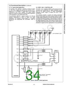
3.7.8 Transmit Outputs
There are two pairs of 10BASE-T output signals. One pair
for Unshielded cable (TXU+/-) and one pair for Shielded
cable (TXS+/-). These two sets of differential outputs are
actually identical to one another. They are both included in
the DP83840A for increased flexibility in multiple media
designs. Note that the characteristic differential cable
impedance for Unshielded cable is 100 Ohms (nominally)
and for Shielded cable is 150 ohms (nominally). Therefore,
special attention must be paid to the external termination
resistor values in order to properly match the 10BASE-T
driver impedance to the load. Refer to Figure 15 for further
detail.
3.7.12 Transmit and Receive Filtering
External 10BASE-T filters are not required when using the
DP83840A as the required signal conditioning is
integrated.
Only isolation/step-up transformers and impedance
matching resistors are required for the 10BASE-T transmit
and receive interface. The internal transmit filtering
ensures that all the harmonics in the transmit signal are
attenuated by at least 30 dB.
Selection between 100 UTP and 150 STP cable operation
is accomplished using the UTP/STP bit in the 10BASE-T
Configuration Register (bit 3, register address 1Ch). Only
one set of outputs is active at any given time. Selecting
UTP will TRI-STATE STP and vice versa.
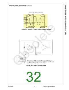
3.7.13 Encoder/Decoder (ENDEC) Module
The Endec Module consists of essentially four functions:
The oscillator generates the 10 MHz transmit clock signal
for system timing from a 20 MHz oscillator.
The TXU+/- and TXS+/- outputs of the DP83840A are
internally filtered and require no additional external
filtering. See Section 3.7.12 for further detail.
Version A
National Semiconductor
30

 TI [ TEXAS INSTRUMENTS ]