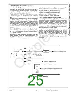
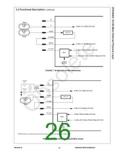
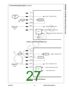
3.0 Functional Description (Continued)
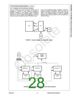
The circuit is shown in Figure 15. Additional output drive
may be necessary if the oscillator must also drive other
components. When using a clock oscillator it is still
recommended that the designer connect the oscillator
output to the X1(OSCIN) pin and leave X2(OSCOUT)
floating
3.6 CLOCK RECOVERY MODULE
The Clock Recovery Module (CRM) is part of the 100 Mb/s
receive channel. The 10 Mb/s clock recovery is
independent from the CRM.
The CRM contains a Phase Locked Loop that tracks the
signal frequency of the incoming 125 Mb/s data stream at
the RD+/- inputs. The CRM extracts a synchronous 125
MHz clock from this data (the data rate on the cable is 125
Mb/s due to 4B5B encoding). The CRM obtains its initial
frequency and stability from its own internal VCO and then
adjusts the frequency as required to match the incoming
data stream frequency. The CRM maintains control of the
PLL's loop gain to minimize the lock time as well as to
minimize the jitter after phase lock has been acquired.
3.7.3 Smart Squelch
The Smart Squelch is responsible for determining when
valid data is present on the differential receive inputs (RXI).
The DP83840A implements an intelligent receive squelch
on the RXI differential inputs to ensure that impulse noise
on the receive inputs will not be mistaken for a valid signal.
Smart squelch operation is independent of the 10BASE-T
operational mode.
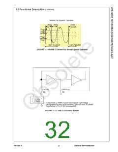
The squelch circuitry employs a combination of amplitude
and timing measurements (as specified in the IEEE 802.3
10BASE-T standard) to determine the validity of data on
the twisted pair inputs (refer to figure 14).
When the Signal Detect (SD+/-) inputs become active, the
CRM attempts to acquire lock. Upon the deassertion of
Signal Detect, the CRM remains locked to the frequency of
the most recent datastream that it had locked to prior to SD
deassertion.
The signal at the start of packet is checked by the smart
squelch and any pulses not exceeding the squelch level
(either positive or negative, depending upon polarity) will
be rejected. Once this first squelch level is overcome cor-
rectly the opposite squelch level must then be exceeded
within 150ns. Finally the signal must exceed the original
squelch level within a further 150ns to ensure that the input
waveform will not be rejected. The checking procedure
results in the loss of typically three bits at the beginning of
each packet.
The CRM generates a 125 MHz clock synchronous with
the receive data stream and presents both the clock and
data to the rest of the 100 Mb/s receive section. The CRM
is not synchronous with the local clock present at the
REFIN input to the CGM.
The RX_CLK signal at the MII interface is derived from the
CRM 125 Mb/s clock during 100 Mb/s operation. The
RX_CLK frequency is set to 25 MHz for nibble-wide receive
data passing to the MAC and/or Repeater.
Only after all these conditions have been satisfied will a
control signal be generated to indicate to the remainder of
the circuitry that valid data is present. At this time, the
smart squelch circuitry is reset.
3.7 10BASE-T TRANSCEIVER MODULE
The 10BASE-T Transceiver Module is IEEE 802.3
compliant. It includes the receiver, transmitter, collision,
heartbeat, loopback, jabber, and link integrity functions, as
defined in the standard. An external filter is not required on
the 10BASE-T interface since this is integrated inside the
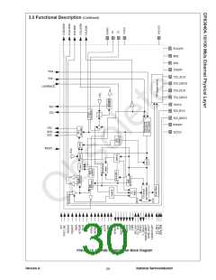
DP83840A. Figure 13 provides a detailed block level
representation of the complete 10BASE-T transceiver
within the DP83840A. Due to the complexity and scope of
the 10BASE-T Transceiver block and various sub-blocks,
this section focuses on the general system level operation.
Valid data is considered to be present until squelch level
has not been generated for a time longer than 150ns,
indicating End of Packet. Once good data has been
detected the squelch levels are reduced to minimize the
effect of noise causing premature End of Packet detection.
The receive squelch threshold level can be lowered for use
in longer cable or STP applications. This is achieved by
setting the LSS bit in the 10BTCR (bit 2, register address
1Ch).
3.7.1 Operational Modes
The DP83840A has 2 basic 10 Mb/s operational modes:
• Half Duplex mode
3.7.4 Collision Detection
For Half Duplex, a 10BASE-T collision is detected when
the receive and transmit channels are active
simultaneously. Collisions are reported by the COL signal
on the MII.
• Full Duplex mode
3.7.1.1 Half Duplex Mode
In Half Duplex mode the DP83840A functions as a
standard IEEE 802.3 10BASE-T transceiver with fully
integrated filtering for both the transmit and receive
10BASE-T signaling (refer to section 3.7).
If the ENDEC is transmitting when a collision is detected,
the collision is not reported until seven bits have been
received while in the collision state. This prevents a
collision being reported incorrectly due to noise on the
network. The COL signal remains set for the duration of the
collision.
3.7.1.2 Full Duplex Mode
In Full Duplex mode the DP83840A is capable of
simultaneously transmitting and receiving without asserting
the collision signal. The DP83840A's 10 Mb/s ENDEC is
designed to encode and decode simultaneously.
When heartbeat is enabled, approximately 1µs after the
transmission of each packet, a Signal Quality Error (SQE)
signal of approximately 10 bit times is generated
(internally) to indicate successful transmission. SQE is
reported as a pulse on the COL signal of the MII.
3.7.2 Oscillator Module Operation
A 20MHz crystal or can-oscillator with the following specifi-
cations is recommended for driving the X1 input.
1.TTL or CMOS output with a 50ppm frequency tolerance
2. 40-60% duty cycle (max).
3.7.5 Carrier Sense
Carrier Sense (CRS) may be asserted due to receive
activity once valid data is detected via the Smart Squelch
function.
3.Two TTL load output drive
Version A
National Semiconductor
28

 TI [ TEXAS INSTRUMENTS ]