3.0 Functional Description (Continued)
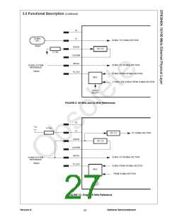
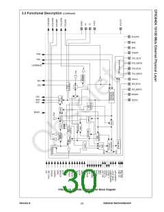
3.5.5.2 Repeater Clock Distribution Example
Due to the demanding timing constraints required to
maintain standards compliance, great care must be
taken in the design and layout of a multi-port repeater
system. The example provided in Figure 12 illustrates
interconnection only and should not be considered as a
reference design.
The clock distribution within a multi-port repeater can be
designed in a variety of ways. Figure 12 provides a
simplified example of one possible timing distribution
scheme in a 100 Mb/s only repeater design. It should be
noted that in order to support Auto-Negotiation, a 20 MHz
reference would be required for each DP83840A device.
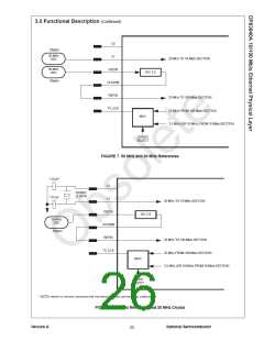
RXD
MAC
PHY
RX_CLK
TD
RD
PMD
TXD
TX_CLK
50
MHz
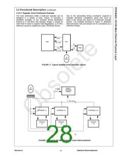
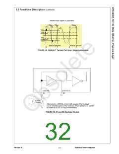
FIGURE 11. Typical Adapter Clock and Data Typical
25
MHz
ENDEC
25 MHz
(DP83850
100RIC)
BUFFER
RX_CLK
DP83840A (1)
DP83840A (2)
DP83840A (12)
DP83223
(1)
DP83223
(2)
DP83223
(12)
FIGURE 12. Typical 100 Mb/s Repeater Clock Interconnection
Version A
National Semiconductor
27

 TI [ TEXAS INSTRUMENTS ]