DM385, DM388
SPRS821D –MARCH 2013–REVISED DECEMBER 2013
www.ti.com
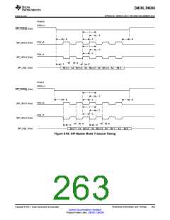
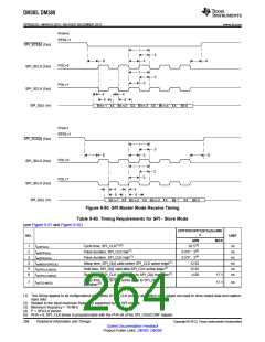
PHA=0
EPOL=1
SPI_SCS[x] (Out)
1
1
3
2
8
2
3
9
POL=0
SPI_SCLK (Out)
POL=1
SPI_SCLK (Out)
4
4
5
5
SPI_D[x] (In)
Bit n-1
Bit n-2
Bit n-3
Bit n-4
Bit 0
PHA=1
EPOL=1
SPI_SCS[x] (Out)
SPI_SCLK (Out)
1
2
1
3
3
2
8
9
POL=0
POL=1
SPI_SCLK (Out)
SPI_D[x] (In)
4
4
5
5
Bit n-1
Bit n-2
Bit n-3
Bit 1
Bit 0
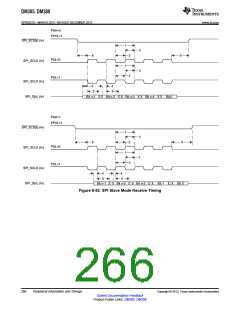
Figure 8-90. SPI Master Mode Receive Timing
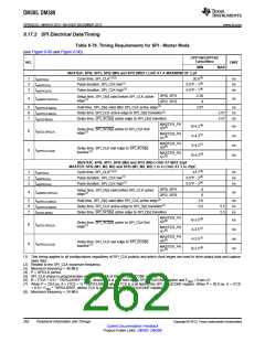
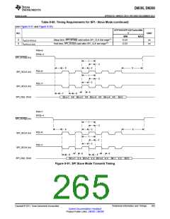
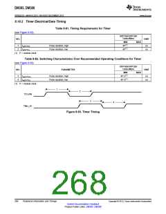
Table 8-80. Timing Requirements for SPI - Slave Mode
(see Figure 8-91 and Figure 8-92)
OPP100/OPP120/Turbo/Nitr
o
NO.
UNIT
MIN
62.5(3)
0.5*P - 3(4)
0.5*P - 3(4)
12.92
MAX
1
2
3
4
5
6
tc(SPICLK)
Cycle time, SPI_CLK(1)(2)
Pulse duration, SPI_CLK low(1)
Pulse duration, SPI_CLK high(1)
Setup time, SPI_D[x] valid before SPI_CLK active edge(1)
Hold time, SPI_D[x] valid after SPI_CLK active edge(1)
Delay time, SPI_CLK active edge to SPI_D[x] transition(1)
ns
ns
ns
ns
ns
ns
tw(SPICLKL)
tw(SPICLKH)
tsu(MOSI-SPICLK)
th(SPICLK-MOSI)
td(SPICLK-MISO)
12.92
-4.00
17.1
17.1
Delay time, SPI_SCS[x] active edge to SPI_D[x]
transition(5)
7
td(SCS-MISO)
ns
(1) This timing applies to all configurations regardless of SPI_CLK polarity and which clock edges are used to drive output data and capture
input data.
(2) Related to the input maximum frequency supported by the SPI module.
(3) Maximum frequency = 16 MHz
(4) P = SPICLK period.
(5) PHA = 0; SPI_CLK phase is programmable with the PHA bit of the SPI_CH(i)CONF register.
264
Peripheral Information and Timings
Copyright © 2013, Texas Instruments Incorporated
Submit Documentation Feedback
Product Folder Links: DM385 DM388

 TI [ TEXAS INSTRUMENTS ]