DM385, DM388
SPRS821D –MARCH 2013–REVISED DECEMBER 2013
www.ti.com
In general, closely coupled differential signal traces are not an advantage on PCBs. When differential
signals are closely coupled, tight spacing and width control is necessary. Very small width and spacing
variations affect impedance dramatically, so tight impedance control can be more problematic to maintain
in production.
Loosely coupled PCB differential signals make impedance control much easier. Wider traces and spacing
make obstacle avoidance easier, and trace width variations do not affect impedance as much; therefore, it
is easier to maintain an accurate impedance over the length of the signal. The wider traces also show
reduced skin effect and, therefore, often result in better signal integrity.
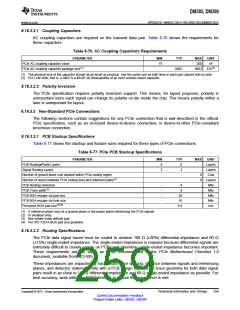
Table 8-78 shows the routing specifications for the PCIe data signals.
Table 8-78. PCIe Routing Specifications
PARAMETER
MIN
TYP
MAX
UNIT
PCIe signal trace length
10(1) Inches
Differential pair trace matching
10(2)
0
Mils
Stubs
Ω
Number of stubs allowed on PCIe traces(3)
TX/RX pair differential impedance
TX/RX single ended impedance
80
51
100
60
120
69
Ω
Pad size of vias on PCIe trace
25(4)
Mils
Mils
Vias(5)
Hole size of vias on PCIe trace
14
Number of vias on each PCIe trace
PCIe differential pair to any other trace spacing
3
2*DS(6)
(1) Beyond this, signal integrity may suffer.
(2) For example, RXP0 within 10 Mils of RXN0.
(3) In-line pads may be used for probing.
(4) 35-Mil antipad max recommended.
(5) Vias must be used in pairs with their distance minimized.
(6) DS = differential spacing of the PCIe traces.
260
Peripheral Information and Timings
Copyright © 2013, Texas Instruments Incorporated
Submit Documentation Feedback
Product Folder Links: DM385 DM388

 TI [ TEXAS INSTRUMENTS ]