DM385, DM388
SPRS821D –MARCH 2013–REVISED DECEMBER 2013
www.ti.com
8.16 Peripheral Component Interconnect Express (PCIe)
The device supports connections to PCIe-compliant devices via the integrated PCIe master/slave bus
interface. The PCIe module is comprised of a dual-mode PCIe core and a SerDes PHY. The device
implements a single one-lane PCIe 2.0 (5.0 GT/s) Endpoint/Root Complex port.
The device PCIe supports the following features:
•
•
•
•
•
•
•
•
•
•
•
•
•
•
Supports Gen1/Gen2 in x1 or x2 mode
One port with one 5 GT/s lane
Single virtual channel (VC), single traffic class (TC)
Single function in end-point mode
Automatic width and speed negotiation and lane reversal
Max payload: 128 byte outbound, 256 byte inbound
Automatic credit management
ECRC generation and checking
Configurable BAR filtering
Supports PCIe messages
Legacy interrupt reception (RC) and generation (EP)
MSI generation and reception
PCI device power management, except D3 cold with vaux
Active state power management state L0 and L1.
For more detailed information on the PCIe port peripheral module, see the PCI Express (PCIe) Module
chapter in the device-specific Technical Reference Manual.
The PCIe peripheral on the device conforms to the PCI Express Base 2.0 Specification.
Note: PCIe is supported on all DM385 devices and also on DM388 devices with PCIe enabled.
8.16.1 PCIe Peripheral Register Descriptions
The PCIe peripheral registers are described in the device-specific Technical Reference Manual. Each
register is documented as an offset from a base address for the peripheral. The base addresses for all of
the peripherals are in the device memory map (see Section 2.10).
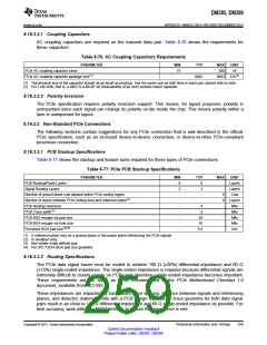
8.16.2 PCIe Electrical Data/Timing
Texas Instruments (TI) has performed the simulation and system characterization to ensure that the PCIe
peripheral meets all AC timing specifications as required by the PCI Express Base 2.0 Specification.
Therefore, the AC timing specifications are not reproduced here. For more information on the AC timing
specifications, see Sections 4.3.3.5 and 4.3.4.4 of the PCI Express Base 2.0 Specification.
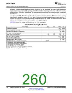
8.16.3 PCIe Design and Layout Guidelines
8.16.3.1 Clock Source
A standard 100-MHz PCIe differential clock source must be used for PCIe operation (for more details, see
Section 7.4.2, SERDES CLKN/P Input Clock).
8.16.3.2 PCIe Connections and Interface Compliance
The PCIe interface on the device is compliant with the PCI Express Base 2.0 Specification. Refer to the
PCIe specifications for all connections that are described in it. For coupling capacitor selection, see
Section 8.16.3.2.1, Coupling Capacitors.
The use of PCIe-compatible bridges and switches is allowed for interfacing with more than one other
processor or PCIe device.
258
Peripheral Information and Timings
Copyright © 2013, Texas Instruments Incorporated
Submit Documentation Feedback
Product Folder Links: DM385 DM388

 TI [ TEXAS INSTRUMENTS ]