DM385, DM388
www.ti.com
SPRS821D –MARCH 2013–REVISED DECEMBER 2013
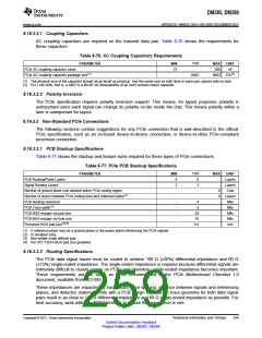
8.16.3.2.1 Coupling Capacitors
AC coupling capacitors are required on the transmit data pair. Table 8-76 shows the requirements for
these capacitors.
Table 8-76. AC Coupling Capacitors Requirements
PARAMETER
MIN
TYP
MAX
200
UNIT
nF
EIA(2)
PCIe AC coupling capacitor value
PCIe AC coupling capacitor package size(1)
75
0402
0603
(1) The physical size of the capacitor should be as small as practical. Use the same size on both lines in each pair, placed side by side.
(2) EIA LxW units; that is, a 0402 is a 40x20 mil (thousandths of an inch) surface-mount capacitor.
8.16.3.2.2 Polarity Inversion
The PCIe specification requires polarity inversion support. This means, for layout purposes, polarity is
unimportant since each signal can change its polarity on-die inside the chip. This means polarity within a
lane is unimportant for layout.
8.16.3.3 Non-Standard PCIe Connections
The following sections contain suggestions for any PCIe connection that is not described in the official
PCIe specification, such as an on-board device-to-device connection, or device-to-other PCIe-compliant
processor connection.
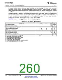
8.16.3.3.1 PCB Stackup Specifications
Table 8-77 shows the stackup and feature sizes required for these types of PCIe connections.
Table 8-77. PCIe PCB Stackup Specifications
PARAMETER
MIN
TYP
6
MAX
UNIT
Layers
Layers
Cuts
Layers
Mils
PCB Routing/Plane Layers
Signal Routing Layers
4
2
-
-
-
3
Number of ground plane cuts allowed within PCIe routing region
Number of layers between PCIe routing area and reference plane(1)
PCB Routing clearance
-
0
0
-
-
-
-
4
PCB Trace width(2)
-
4
-
Mils
PCB BGA escape via pad size
-
20
10
0.4
-
Mils
PCB BGA escape via hole size
Processor BGA pad size(3)(4)
-
Mils
mm
(1) A reference plane may be a ground plane or the power plane referencing the PCIe signals.
(2) In breakout area.
(3) Non-solder mask defined pad.
(4) Per IPC-7351A BGA pad size guideline.
8.16.3.3.2 Routing Specifications
The PCIe data signal traces must be routed to achieve 100 Ω (±20%) differential impedance and 60 Ω
(±15%) single-ended impedance. The single-ended impedance is required because differential signals are
extremely difficult to closely couple on PCBs and, therefore, single-ended impedance becomes important.
These requirements are the same as those recommended in the PCIe Motherboard Checklist 1.0
document, available from PCI-SIG.
These impedances are impacted by trace width, trace spacing, distance between signals and referencing
planes, and dielectric material. Verify with a PCB design tool that the trace geometry for both data signal
pairs result in as close to 100 Ω differential impedance and 60 Ω single-ended impedance as possible. For
best accuracy, work with your PCB fabricator to ensure this impedance is met.
Copyright © 2013, Texas Instruments Incorporated
Peripheral Information and Timings
259
Submit Documentation Feedback
Product Folder Links: DM385 DM388

 TI [ TEXAS INSTRUMENTS ]