DM385, DM388
www.ti.com
SPRS821D –MARCH 2013–REVISED DECEMBER 2013
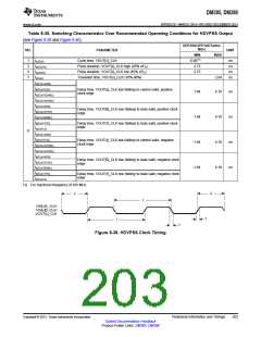
8.10.3 Video HD-DAC Guidelines and Electrical Data/Timing
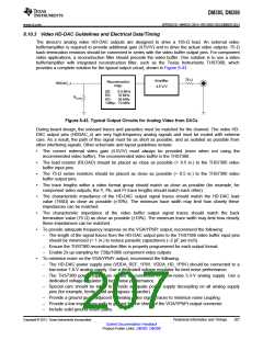
The device's analog video HD-DAC outputs are designed to drive a 165-Ω load. An external video
buffer/amplifier is required to provide additional gain (4.5V/V) and to drive the actual video outputs. 75-Ω
back termination resistors should be connected in series with the video buffer output pins. For component
video applications, a reconstruction filter should precede the video buffer. One solution is to use a video
buffer/amplifier with integrated reconstruction filter, such as the Texas Instruments THS7360, which
provides a complete solution for the typical output circuit, shown in Figure 8-43.
75 W
Amplifier
4.5 V/V
Reconstruction
Filter
HDDAC_x
SD:
ED:
HD:
9.5 MHz
18 MHz
36 MHz
RLOAD
1080p: 72 MHz
Figure 8-43. Typical Output Circuits for Analog Video from DACs
During board design, the onboard traces and parasitics must be matched for the channel. The video HD-
DAC output pins (HDDAC_x) are very high-frequency analog signals and must be routed with extreme
care. As a result, the path of this signal must be as short as possible, and as isolated as possible from
other interfering signals. Other schematic and layout guidelines include:
•
•
•
•
•
The correct external video gain (4.5V/V) must always be provided (even when not using the
recommended video buffer). The recommended video buffer is the THS7360.
The load resistor (RLOAD) should be placed as close as possible (< 0.5 in.) to the THS7360 video
buffer input pins.
The 75-Ω series resistors should be placed as close as possible (< 0.5 in.) to the THS7360 video
buffer output pins.
The trace lengths within a video format group should match as close as possible (for example, for
component video outputs, the Y, Pb, and Pr trace lengths should match each other).
The characteristic impedance of the HD-DAC output signal traces should match the HD-DAC load
value (165Ω) as close as possible (±10%). The minimum trace width may limit how closely these
impedances can be matched.
•
•
The characteristic impedance of the video buffer output signal traces should match the back
termination value (75 Ω) as close as possible (±10%). The minimum trace width may limit how closely
these impedances can be matched.
To provide adequate frequency response on the VGA/YPbPr output, recommend the following:
–
The length of the signal traces from the HD-DAC output pins to the THS7360 video buffer input pins
should be minimized (< 1 in.) to reduce parasitic capacitance (~2 pF per inch).
–
–
Ensure the THS7360 reconstruction filter is properly programmed for each output format.
Enable 2x up-sampling for 720p/1080i component video outputs.
•
To minimize noise on the VGA/YPbPr output, recommend the following:
–
–
–
The HD-DAC power supply pins (VDDA_REF_1P8V, VDDA_HD_1P8V) should be connected to a
low-noise 1.8-V analog supply. Use a dedicated voltage regulator for best noise performance.
The THS7360 power supply pin should be connected to a low-noise 3.3-V analog supply. Use a
dedicated voltage regulator for best noise performance.
Special care should be taken to provide adequate power supply decoupling on all analog supply
pins (for example, ferrite bead and bypass capacitor).
–
–
–
Provide a ground guard adjacent to analog video signal traces to minimize noise coupling.
Provide a low impedance path to ground for the shield of the VGA/YPbPr output connector.
Include solid ground return paths.
Copyright © 2013, Texas Instruments Incorporated
Peripheral Information and Timings
207
Submit Documentation Feedback
Product Folder Links: DM385 DM388

 TI [ TEXAS INSTRUMENTS ]