DM385, DM388
www.ti.com
SPRS821D –MARCH 2013–REVISED DECEMBER 2013
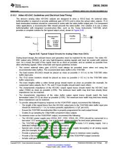
8.10.2 Video SD-DAC Guidelines and Electrical Data/Timing
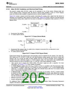
The device's analog video SD-DAC output can be operated in one of two modes: Normal mode and
TVOUT Bypass mode. In Normal mode, the device’s internal video amplifier is used. In TVOUT Bypass
mode, the internal video amplifier is bypassed and an external amplifier is required.
Figure 8-41 shows a typical circuit that permits connecting the analog video output from the device to
standard 75-Ω impedance video systems in Normal mode. Figure 8-42 shows a typical circuit that permits
connecting the analog video output from the device to standard 75-Ω impedance video systems in TVOUT
Bypass mode.
Reconstruction
Filter(A)
~9.5 MHz
TV_OUTx
(B)
CAC
ROUT
TV_VFBx
A. Reconstruction Filter (optional)
B. AC coupling capacitor (optional)
Figure 8-41. TV Output (Normal Mode)
75 Ω
Reconstruction
Filter(A)
~9.5 MHz
Amplifier
3.7 V/V
TV_VFBx
(B)
CAC
RLOAD
A. Reconstruction Filter (optional). Note: An amplifier with an integrated reconstruction filter can alternatively be used
instead of a discrete reconstruction filter.
B. AC coupling capacitor (optional)
Figure 8-42. TV Output (TVOUT Bypass Mode)
During board design, the onboard traces and parasitics must be matched for the channel. The video SD-
DAC output pin (TV_OUT0/TV_VFB0) are very high-frequency analog signals and must be routed with
extreme care. As a result, the paths of these signals must be as short as possible, and as isolated as
possible from other interfering signals. In TVOUT Bypass mode, the load resistor and amplifier/buffer
should be placed as close as possible to the TV_VFB0 pin. Other layout guidelines include:
•
Take special care to bypass the VDDA_VDAC_1P8 power supply pin with a capacitor. For more
information, see Section 7.2.9, Power-Supply Decoupling.
•
In TVOUT Bypass mode, place the RLOAD resistor as close as possible to the Reconstruction Filter
and Amplifier. In addition, place the 75-Ω resistor as close as possible (< 0.5 ") to the Amplifier/buffer
output pin. To maintain a high-quality video signal, the onboard traces after the 75-Ω resistor should
have a characteristic impedance of 75 Ω (± 20%).
•
In Normal mode, TV_VFB0 is the most sensitive pin in the TV out system. The ROUT resistor should
be placed as close as possible to the device pin. To maintain a high-quality video signal, the onboard
traces leading to the TV_OUT0 pin should have a characteristic impedance of 75 Ω (± 20%) starting
from the closest possible place to the device pin output.
•
•
Minimize input trace lengths to the device to reduce parasitic capacitance.
Include solid ground return paths.
For additional Video SD-DAC Design guidelines, see the High Definition Video Processing Subsystem
chapter in the device-specific Technical Reference Manual.
Copyright © 2013, Texas Instruments Incorporated
Peripheral Information and Timings
205
Submit Documentation Feedback
Product Folder Links: DM385 DM388

 TI [ TEXAS INSTRUMENTS ]