DM385, DM388
www.ti.com
SPRS821D –MARCH 2013–REVISED DECEMBER 2013
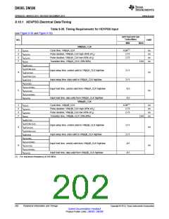
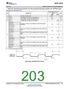
Table 8-36. Switching Characteristics Over Recommended Operating Conditions for HDVPSS Output
(see Figure 8-38 and Figure 8-40)
OPP100/OPP120/Turbo/
Nitro
NO.
PARAMETER
UNIT
MIN
MAX
1
2
3
7
tc(CLK)
Cycle time, VOUT[x]_CLK
6.06(1)
2.73
ns
ns
ns
ns
tw(CLKH)
Pulse duration, VOUT[x]_CLK high (45% of tc)
Pulse duration, VOUT[x]_CLK low (45% of tc)
Transition time, VOUT[x]_CLK (10%-90%)
tw(CLKL)
2.73
tt(CLK)
2.64
4.18
td(CLK-AVID)
td(CLK-FLD)
td(CLK-VSYNC)
td(CLK-HSYNC)
td(CLK-RCR)
td(CLK-GYYC)
td(CLK-BCBC)
td(CLK-YYC)
td(CLK-C)
Delay time, VOUT[x]_CLK low (falling) to control valid, positive
clock edge
1.64
1.64
ns
ns
ns
ns
Delay time, VOUT[0]_CLK low (falling) to data valid, positive clock
edge
4.18
4.18
4.18
Delay time, VOUT[1]_CLK low (falling) to data valid, positive clock
edge
6
td(CLK-AVID)
td(CLK-FLD)
td(CLK-VSYNC)
td(CLK-HSYNC)
td(CLK-RCR)
td(CLK-GYYC)
td(CLK-BCBC)
td(CLK-YYC)
td(CLK-C)
Delay time, VOUT[x]_CLK low (falling) to control valid, negative
clock edge
-1.64
-1.64
Delay time, VOUT[0]_CLK low (falling) to data valid, negative clock
edge
Delay time, VOUT[1]_CLK low (falling) to data valid, negative clock
edge
(1) For maximum frequency of 165 MHz.
3
2
1
VIN[x]A_CLK/
VIN[x]B_CLK/
VOUT[x]_CLK
7
1
7
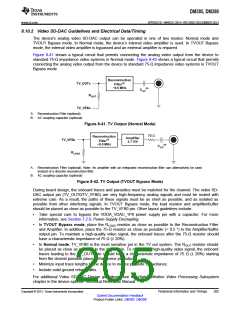
Figure 8-38. HDVPSS Clock Timing
Copyright © 2013, Texas Instruments Incorporated
Peripheral Information and Timings
203
Submit Documentation Feedback
Product Folder Links: DM385 DM388

 TI [ TEXAS INSTRUMENTS ]