DM385, DM388
SPRS821D –MARCH 2013–REVISED DECEMBER 2013
www.ti.com
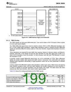
Table 8-33. TMDS Routing Specifications (continued)
PARAMETER
Number of vias on each TMDS trace
MIN
TYP
MAX
UNIT
Vias(1)
2
TMDS differential pair to any other trace spacing
2*DS(2)
(1) Vias must be used in pairs with their distance minimized.
(2) DS = differential spacing of the HDMI traces.
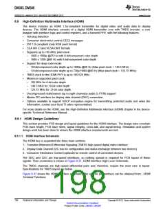
8.9.1.3 DDC Signals
As shown in Figure 8-37, HDMI Interface High-Level Schematic, the DDC connects just like a standard
I2C bus. As such, resistor pullups must be used to pull up the open drain buffer signals unless they are
integrated into the ESD protection chip used. If used, these pullup resistors should be connected to a 3.3-
V supply.
8.9.1.4 HDMI ESD Protection Device (Required)
Interfaces that connect to a cable such as HDMI generally require more ESD protection than can be built
into the processor's outputs. Therefore, this HDMI interface requires the use of an ESD protection chip to
provide adequate ESD protection and to translate I2C voltage levels from the 3.3 V supplied by the device
to the 5 volts required by the HDMI specification.
When selecting an ESD protection chip, choose the lowest capacitance ESD protection available to
minimize signal degradation. In no case should the ESD protection circuit capacitance be more than 5 pF.
TI manufactures devices that provide ESD protection for HDMI signals such as the TPD12S521. For more
information see the www.ti.com website.
8.9.1.5 PCB Stackup Specifications
Table 8-34 shows the stackup and feature sizes required for HDMI.
Table 8-34. HDMI PCB Stackup Specifications
PARAMETER
MIN
TYP
6
MAX
UNIT
Layers
Layers
Cuts
PCB routing/plane layers
Signal routing layers
4
2
-
-
-
3
Number of ground plane cuts allowed within HDMI routing region
Number of layers between HDMI routing region and reference ground plane
PCB trace width
-
0
0
-
-
-
Layers
Mils
-
4
PCB BGA escape via pad size
-
20
10
0.4
-
Mils
PCB BGA escape via hole size
Processor device BGA pad size(1)(2)
-
Mils
mm
(1) Non-solder mask defined pad.
(2) Per IPC-7351A BGA pad size guideline.
8.9.1.6 Grounding
Each TMDS channel has its own shield pin which should be grounded to provide a return current path for
the TMDS signal.
200
Peripheral Information and Timings
Copyright © 2013, Texas Instruments Incorporated
Submit Documentation Feedback
Product Folder Links: DM385 DM388

 TI [ TEXAS INSTRUMENTS ]