DM385, DM388
www.ti.com
SPRS821D –MARCH 2013–REVISED DECEMBER 2013
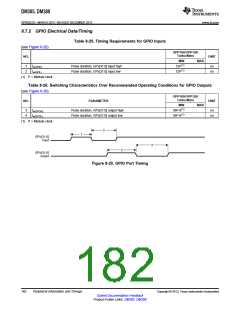
8.7 General-Purpose Input/Output (GPIO)
The GPIO peripheral provides general-purpose pins that can be configured as either inputs or outputs.
When configured as an output, a write to an internal register controls the state driven on the output pin.
When configured as an input, the state of the input is detectable by reading the state of an internal
register. In addition, the GPIO peripheral can produce CPU interrupts in different interrupt generation
modes. The GPIO peripheral provides generic connections to external devices.
The device contains four GPIO modules and each GPIO module consists of up to 32 identical channels.
The device GPIO peripheral supports the following:
•
Up to 125 1.8-V/3.3-V GPIO pins, GP0[0:28], GP1[0:31], GP2[0:31], and GP3[0:31] (the exact number
available varies as a function of the device configuration). Each channel can be configured to be used
in the following applications:
–
–
–
Data input/output
Keyboard interface with a de-bouncing cell
Synchronous interrupt generation (in active mode) upon the detection of external events (signal
transitions and/or signal levels).
•
•
Synchronous interrupt requests from each channel are processed by four identical interrupt generation
sub-modules to be used independently by the ARM or Media Controller. Interrupts can be triggered by
rising and/or falling edge, specified for each interrupt-capable GPIO signal.
Shared registers can be accessed through "Set & Clear" protocol. Software writes 1 to corresponding
bit positions to set or to clear GPIO signals. This allows multiple software processes to toggle GPIO
output signals without critical section protection (disable interrupts, program GPIO, re-enable interrupts,
to prevent context switching to another process during GPIO programming).
•
•
Separate input/output registers.
Output register in addition to set/clear so that, if preferred by software, some GPIO output signals can
be toggled by direct write to the output registers.
•
Output register, when read, reflects output drive status. This, in addition to the input register reflecting
pin status and open-drain I/O cell, allows wired logic to be implemented.
For more detailed information on GPIOs, see the General-Purpose I/O (GPIO) Interface chapter in the
device-specific Technical Reference Manual.
8.7.1 GPIO Peripheral Register Descriptions
The GPIO peripheral registers are described in the device-specific Technical Reference Manual. Each
register is documented as an offset from a base address for the peripheral. The base addresses for all of
the peripherals are in the device memory map (see Section 2.10).
Copyright © 2013, Texas Instruments Incorporated
Peripheral Information and Timings
181
Submit Documentation Feedback
Product Folder Links: DM385 DM388

 TI [ TEXAS INSTRUMENTS ]