DM385, DM388
SPRS821D –MARCH 2013–REVISED DECEMBER 2013
www.ti.com
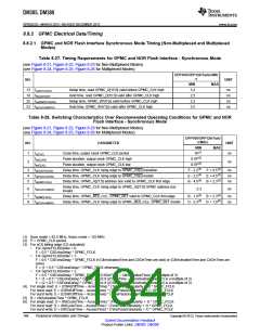
8.8.2 GPMC Electrical Data/Timing
8.8.2.1 GPMC and NOR Flash Interface Synchronous Mode Timing (Non-Multiplexed and Multiplexed
Modes)
Table 8-27. Timing Requirements for GPMC and NOR Flash Interface - Synchronous Mode
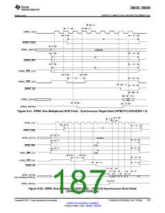
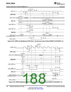
(see Figure 8-21, Figure 8-22, Figure 8-23 for Non-Multiplexed Modes)
(see Figure 8-24, Figure 8-25, Figure 8-26 for Multiplexed Modes)
OPP100/OPP120/Turbo/Nitr
o
NO.
UNIT
MIN
3.2
2.5
3.2
2.5
MAX
13 tsu(DV-CLKH)
14 th(CLKH-DV)
22 tsu(WAITV-CLKH)
23 th(CLKH-WAITV)
Setup time, read GPMC_D[15:0] valid before GPMC_CLK high
Hold time, read GPMC_D[15:0] valid after GPMC_CLK high
Setup time, GPMC_WAIT[x] valid before GPMC_CLK high
Hold time, GPMC_WAIT[x] valid after GPMC_CLK high
ns
ns
ns
ns
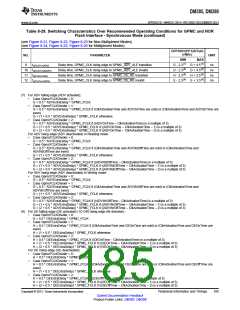
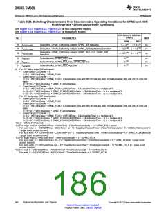
Table 8-28. Switching Characteristics Over Recommended Operating Conditions for GPMC and NOR
Flash Interface - Synchronous Mode
(see Figure 8-21, Figure 8-22, Figure 8-23 for Non-Multiplexed Modes)
(see Figure 8-24, Figure 8-25, Figure 8-26 for Multiplexed Modes)
OPP100/OPP120/Turb
o/Nitro
NO.
PARAMETER
UNIT
MIN
MAX
1
2
tc(CLK)
Cycle time, output clock GPMC_CLK period
16(1)
0.5P(2)
0.5P(2)
ns
ns
tw(CLKH)
Pulse duration, output clock GPMC_CLK high
tw(CLKL)
Pulse duration, output clock GPMC_CLK low
3
4
5
td(CLKH-nCSV)
td(CLKH-nCSIV)
td(ADDV-CLK)
Delay time, GPMC_CLK rising edge to GPMC_CS[x] transition
Delay time, GPMC_CLK rising edge to GPMC_CS[x] invalid
Delay time, GPMC_A[27:0] address bus valid to GPMC_CLK first edge
F - 2.2(3) F + 4.5(3)
E - 2.2(4) E + 4.5(4)
B - 4.5(5) B + 2.3(5)
ns
ns
ns
Delay time, GPMC_CLK rising edge to GPMC_A[27:0] GPMC address bus
invalid
6
td(CLKH-ADDIV)
-2.3
ns
7
8
td(nBEV-CLK)
Delay time, GPMC_BE0_CLE, GPMC_BE1 valid to GPMC_CLK first edge
Delay time, GPMC_CLK rising edge to GPMC_BE0_CLE, GPMC_BE1 invalid
B - 1.9(5) B + 2.3(5)
D - 2.3(6) D + 1.9(6)
ns
ns
td(CLKH-nBEIV)
(1) Sync mode = 62.5 MHz; Async mode = 125 MHz.
(2) P = GPMC_CLK period.
(3) For nCS falling edge (CS activated):
•
For GpmcFCLKDivider = 0:
F = 0.5 * CSExtraDelay * GPMC_FCLK
For GpmcFCLKDivider = 1:
•
F = 0.5 * CSExtraDelay * GPMC_FCLK if (ClkActivationTime and CSOnTime are odd) or (ClkActivationTime and CSOnTime are
even)
F = (1 + 0.5 * CSExtraDelay) * GPMC_FCLK otherwise
•
For GpmcFCLKDivider = 2:
F = 0.5 * CSExtraDelay * GPMC_FCLK if ((CSOnTime – ClkActivationTime) is a multiple of 3)
F = (1 + 0.5 * CSExtraDelay) * GPMC_FCLK if ((CSOnTime – ClkActivationTime – 1) is a multiple of 3)
F = (2 + 0.5 * CSExtraDelay) * GPMC_FCLK if ((CSOnTime – ClkActivationTime – 2) is a multiple of 3)
(4) For single read: E = (CSRdOffTime – AccessTime) * (TimeParaGranularity + 1) * GPMC_FCLK
For burst read: E = (CSRdOffTime – AccessTime) * (TimeParaGranularity + 1) * GPMC_FCLK
For burst write: E = (CSWrOffTime – AccessTime) * (TimeParaGranularity + 1) * GPMC_FCLK
(5) B = ClkActivationTime * GPMC_FCLK
(6) For single read: D = (RdCycleTime – AccessTime) * (TimeParaGranularity + 1) * GPMC_FCLK
For burst read: D = (RdCycleTime – AccessTime) * (TimeParaGranularity + 1) * GPMC_FCLK
For burst write: D = (WrCycleTime – AccessTime) * (TimeParaGranularity + 1) * GPMC_FCLK
184
Peripheral Information and Timings
Copyright © 2013, Texas Instruments Incorporated
Submit Documentation Feedback
Product Folder Links: DM385 DM388

 TI [ TEXAS INSTRUMENTS ]