DM385, DM388
SPRS821D –MARCH 2013–REVISED DECEMBER 2013
www.ti.com
NOTE
The reset pin state is after all the power supplies are ramped up and stable. The state is not
not ensured during power-up sequencing.
Upon coming out of reset, the ARM Cortex-A8 starts executing code from the internal Boot
ROM. The Boot ROM code modifies the PINCNTLx registers to configure the associated
pins for the chosen primary and backup Bootmodes.
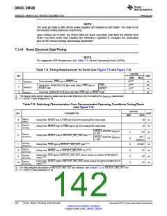
7.3.18 Reset Electrical Data/Timing
NOTE
For supported OPP frequencies, see Table 7-3, Device Operating Points (OPPs).
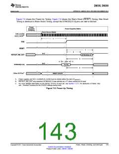
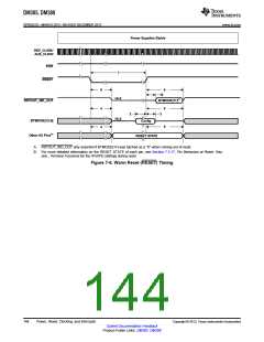
Table 7-8. Timing Requirements for Reset (see Figure 7-5 and Figure 7-6)
OPP100
NO.
1
UNIT
MIN
12P(1)
2P(2)
2P(2)
0
MAX
tw(RESET)
tsu(BOOT)
th(BOOT)
Pulse duration, POR low or RESET low
ns
ns
ns
ns
POR
Setup time, BTMODE[15:0] pins valid before POR high or
RESET high
2
RESET
3
Hold time, BTMODE[15:0] pins valid after POR high or RESET high
(1) The device clock source must be stable and at a valid frequency prior to meeting the tw(RESET) requirement.
(2) P = 1/(DEV Clock) frequency in ns.
Table 7-9. Switching Characteristics Over Recommended Operating Conditions During Reset
(see Figure 7-6)
OPP100
NO.
PARAMETER
UNIT
MIN
MAX
td(RSTL-
IORST)
4
5
Delay time, RESET low or POR low to all I/Os entering their reset state
Delay time, RESET high or POR high to all I/Os exiting their reset state
14 ns
td(RSTH-
IOFUNC)
14 ns
2P ns
RESET assertion tw(RESET)
0
0
0
0
0
0
≥ 30P
td(RSTH-
RSTOUTH)
6
Delay time, RESET high to RSTOUT_WD_OUT high(1)(2)
RESET assertion tw(RESET)
< 30P
32P -
tw(RESET)
ns
td(PORH-
RSTOUTH)
td(RSTL-
RSTOUTZ)
td(PORH-
RSTOUTL)
td(RSTH-
RSTOUTD)
7
8
Delay time, POR high to RSTOUT_WD_OUT high(1)(2)
Delay time, RESET low to RSTOUT_WD_OUT Hi-Z(1)(2)
12500P ns
2P ns
Delay time, POR high to RSTOUT_WD_OUT driven based on latched BTMODE[11]
value(1)(2)
9
2P ns
Delay time, RESET high to RSTOUT_WD_OUT driven based on latched BTMODE[11]
value(1)(2)
10
2P ns
(1) For more detailed information on RSTOUT_WD_OUT pin behavior, see Section 7.3.14, RSTOUT_WD_OUT Pin.
(2) P = 1/(DEV Clock) frequency in ns.
142
Power, Reset, Clocking, and Interrupts
Copyright © 2013, Texas Instruments Incorporated
Submit Documentation Feedback
Product Folder Links: DM385 DM388

 TI [ TEXAS INSTRUMENTS ]