DM385, DM388
www.ti.com
SPRS821D –MARCH 2013–REVISED DECEMBER 2013
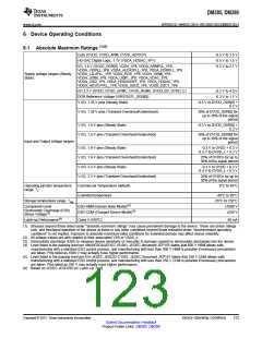
6 Device Operating Conditions
(1)(2)
6.1 Absolute Maximum Ratings
Core (CVDD, CVDD_ARM, CVDD_HDVICP)
HD-DAC Digital Logic, 1.1V (VDDA_HDDAC_1P1)
-0.3 V to 1.5 V
-0.5 V to 1.5 V
I/O, 1.8 V (DVDD_DDR[0], VDDA_1P8, VDDA_ARMPLL_1P8,
VDDA_VIDPLL_1P8, VDDA_AUDIOPLL_1P8, VDDA_DDRPLL_1P8,
VDDA_L3L4PLL_1P8, VDDA_PCIE_1P8, VDDA_HDMI_1P8,
VDDA_USB0_1P8, VDDA_USB1_1P8, VDDA_VDAC_1P8,
VDDA_CSI2_1P8, VDDA_HDDACREF_1P8, VDDA_HDDAC_1P8,
VDDA_HDVICPPLL_1P8, VDDS_OSC0_1P8, VDDS_OSC1_1P8
-0.3 V to 2.1 V
Supply voltage ranges (Steady
State):
I/O 3.3 V (DVDD, DVDD_GPMC, DVDD_RGMII, DVDD_SD, DVDD_C)
DDR Reference Voltage (VREFSSTL_DDR[0])
V I/O, 1.35-V pins (Steady State)
-0.3 V to 4.0 V
-0.3 V to 1.1 V
-0.3 V to DVDD_DDR[0] +
0.3 V
V I/O, 1.35-V pins (Transient Overshoot/Undershoot)
30% of DVDD_DDR[0] for
up to 30% of the signal
period
V I/O, 1.5-V pins (Steady State)
-0.3 V to DVDD_DDR[0] +
0.3 V
V I/O, 1.5-V pins (Transient Overshoot/Undershoot)
30% of DVDD_DDR[0] for
up to 30% of the signal
period
Input and Output voltage ranges:
V I/O, 1.8-V pins (Steady State)
-0.3 V to DVDD + 0.3 V
-0.3 V to DVDD_x + 0.3 V
V I/O, 1.8-V pins (Transient Overshoot/Undershoot)
V I/O, 3.3-V pins (Steady State)
25% of DVDDx for up to
30% of the signal period
-0.3 V to DVDD + 0.3 V
-0.3 V to DVDD_x + 0.3 V
V I/O, 3.3-V pins (Transient Overshoot/Undershoot)
Commercial Temperature (default)
Extended temperature
25% of DVDDx for up to
30% of the signal period
Operating junction temperature
range, TJ:
0°C to 95°C
-40°C to 95°C
-55°C to 150°C
±1000 V
Storage temperature range, Tstg
:
Component-Level
ESD-HBM (Human Body Model)(4)
ESD-CDM (Charged-Device Model)(5)
Electrostatic Discharge (ESD)
±250 V
Stress Voltage(3)
Latch-up Performance(6)
Class II (105ºC)
50 mA
(1) Stresses beyond those listed under "absolute maximum ratings" may cause permanent damage to the device. These are stress ratings
only, and functional operation of the device at these or any other conditions beyond those indicated under "recommended operating
conditions" is not implied. Exposure to absolute-maximum-rated conditions for extended periods may affect device reliability.
(2) All voltage values are with respect to their associated VSS or VSSA_x.
(3) Electrostatic discharge (ESD) to measure device sensitivity or immunity to damage caused by electrostatic discharges into the device.
(4) Level listed is the passing level per ANSI/ESDA/JEDEC JS-001. JEDEC document JEP155 states that 500 V HBM allows safe
manufacturing with a standard ESD control process, and manufacturing with less than 500 V HBM is possible if necessary precautions
are taken. Pins listed as 1000 V may actually have higher performance.
(5) Level listed is the passing level per EIA-JEDEC JESD22-C101E. JEDEC document JEP157 states that 250 V CDM allows safe
manufacturing with a standard ESD control process, and manufacturing with less than 250 V CDM is possible if necessary precautions
are taken. Pins listed as 250 V may actually have higher performance.
(6) Based on JEDEC JESD78D [IC Latch-Up Test].
Copyright © 2013, Texas Instruments Incorporated
Device Operating Conditions
123
Submit Documentation Feedback
Product Folder Links: DM385 DM388

 TI [ TEXAS INSTRUMENTS ]