DM385, DM388
SPRS821D –MARCH 2013–REVISED DECEMBER 2013
www.ti.com
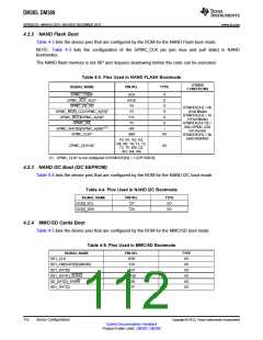
4.2.2 NAND Flash Boot
Table 4-3 lists the device pins that are configured by the ROM for the NAND Flash boot mode.
NOTE: Table 4-3 lists the configuration of the GPMC_CLK pin (pin mux and pull state) in NAND
bootmodes.
The NAND flash memory is not XIP and requires shadowing before the code can be executed.
Table 4-3. Pins Used in NAND FLASH Bootmode
OTHER
CONDITIONS
SIGNAL NAME
PIN NO.
TYPE
GPMC_CS[0]/*
GPMC_ADV_ALE/*
AC9
AA10
Y8
O
O
O
O
O
O
I
GPMC_OE_RE
BTMODE[12] = 0b
(8-bit Mode)
BTMODE[12] = 1b
(16-bit Mode)
GPMC_BE[0]_CLE/GPMC_A[25]/*
GPMC_BE[1]/GPMC_A[24]/*
GPMC_WE
Y3
Y11
Y5
BTMODE[14:13] =
00b (GPMC CS0
not muxed)
BTMODE[15] = 0b
(wait disabled)
GPMC_WAIT[0]/GPMC_A[26]/*(1)
W8
GPMC_CLK/*
AB9
I/O
P2, R1, R2, R3,
R4, R6, T8, T1, T2,
T3, T5, W9, U2,
W3, W4, W6
GPMC_D[15:0]/*
I/O
(1) GPMC_CLK/* is not configured in BTMODE[10] = 1 [OPTION B]
4.2.3 NAND I2C Boot (I2C EEPROM)
Table 4-4 lists the device pins that are configured by the ROM for the NAND I2C boot mode.
Table 4-4. Pins Used in NAND I2C Bootmode
SIGNAL NAME
I2C[0]_SCL
I2C[0]_SDA
PIN NO.
T27
TYPE
I/O
T24
I/O
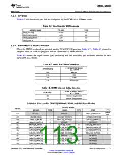
4.2.4 MMC/SD Cards Boot
Table 4-5 lists the device pins that are configured by the ROM for the MMC/SD boot mode.
Table 4-5. Pins Used in MMC/SD Bootmode
SIGNAL NAME
SD1_CLK
PIN NO.
W30
Y29
TYPE
I/O
SD1_CMD/GP0[0] [MUX0]
SD1_DAT[0]
I/O
W31
AA30
U29
I/O
SD1_DAT[1]_SDIRQ
SD_DAT[2]_SDRW
SD1_DAT[3]
I/O
I/O
Y27
I/O
112
Device Configurations
Copyright © 2013, Texas Instruments Incorporated
Submit Documentation Feedback
Product Folder Links: DM385 DM388

 TI [ TEXAS INSTRUMENTS ]