DM385, DM388
www.ti.com
SPRS821D –MARCH 2013–REVISED DECEMBER 2013
4.3 Pin Multiplexing Control
Device level pin multiplexing is controlled on a pin-by-pin basis by the MUXMODE bits of the PINCNTL1 –
PINCNTL270 registers in the Control Module.
Pin multiplexing selects which one of several peripheral pin functions controls the pin's I/O buffer output
data values. Table 4-12 shows the peripheral pin functions associated with each MUXMODE setting for all
multiplexed pins. The default pin multiplexing control for almost every pin is to select MUXMODE = 0x0, in
which case the pin's I/O buffer is 3-stated.
In most cases, the input from each pin is routed to all of the peripherals that share the pin, regardless of
the MUXMODE setting. However, in some cases a constant "0" or "1" value is routed to the associated
peripheral when its peripheral function is not selected to control any output pin. For more details on the
De-Selected Input State (DSIS), see the columns of each Terminal Functions table (Section 3.3, Terminal
Functions).
Some peripheral pin functions can be routed to more than one device pin. These types of peripheral pin
functions are called Multimuxed and may have different Switching Characteristics and Timing
Requirements for each device pin option.
For more detailed information on the Pin Control 1 through Pin Control 270 (PINCNTLx) registers
breakout, see Figure 4-1 and Table 4-12.
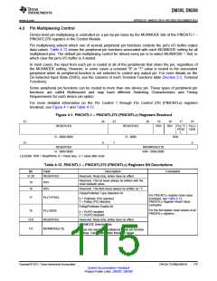
Figure 4-1. PINCNTL1 – PINCNTL270 (PINCNTLx) Registers Breakout
31
15
24
23
20
19
18
17
16
RESERVED
RESERVED
R - 0000
RSV
RSV PLLTY PLLU
PESE
L
DEN
R - 0000 0000
R/W
8
7
0
RESERVED
MUXMODE[7:0]
R/W - 0000 0000
R - 0000 0000
LEGEND: R/W = Read/Write; R = Read only; -n = value after reset
Table 4-12. PINCNTL1 – PINCNTL270 (PINCNTLx) Registers Bit Descriptions
Bit
Field
Description
Comments
31:20
RESERVED
Reserved. Read only, writes have no effect.
Reserved. This bit must always be written with the
reset (default) value.
19
18
RSV
RSV
Reserved. This field must always be written as "1".
Pullup/Pulldown Type Selection bit
For PINCNTLx register reset value
examples, see Table 4-13,
PNICNTLx Register Reset Value
Examples.
17
PLLTYPSEL
0 = Pulldown (PD) selected
1 = Pullup (PU) selected
Pullup/Pulldown Enable bit
For the full register reset values of all
PINCNTLx registers.
16
15:8
7:0
PLLUDEN
0 = PU/PD enabled
1 = PU/PD disabled
RESERVED
MUXMODE[7:0]
Reserved. Read only, writes have no effect.
MUXMODE Selection bits
These bits select the multiplexed mode pin function
settings. Values other than those are illegal.
Copyright © 2013, Texas Instruments Incorporated
Device Configurations
115
Submit Documentation Feedback
Product Folder Links: DM385 DM388

 TI [ TEXAS INSTRUMENTS ]