DLPA2000
ZHCSCO5B –JUNE 2014–REVISED FEBRUARY 2018
www.ti.com.cn
MAX UNIT
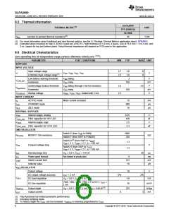
Electrical Characteristics (continued)
over operating free-air temperature range (unless otherwise noted) (see (1)(2)
)
PARAMETER
VBIAS REGULATOR
TEST CONDITIONS
MIN
TYP
Output voltage
18
V
DC output voltage accuracy
DC load regulation
IOUT = 2 mA
–2%
2%
VBIAS
VIN = 3.6 V, IOUT = 0 to 2 mA
–14
18
V/A
VINA, VINL, VINR, VINC 2.7 to 6 V,
IOUT = 2 mA
DC line regulation
mV/V
mVpp
VIN = 3.6 V, IOUT = 2 mA, COUT = 440 nF
VRIPPLE
IOUT
Output ripple
375
(3)
(see
)
Output current
0
4
mA
Power-good threshold
(fraction of nominal output
voltage)
VBIAS rising
86%
66%
100
PG
VBIAS falling
RDIS
Output discharge resistor
Active when rail is disabled
Ω
Recommended value (output capacitors for
VOFS / VBIAS must be equal)
110
100
220
COUT
Output capacitor
nF
tDISCHARGE < 40 µs at 2.9 V
110
3%
VRST REGULATOR
Output voltage
–14
V
DC output voltage accuracy
DC load regulation
IOUT = 2 mA
–3%
VRST
VIN = 3.6 V, IOUT = 0 to 2 mA
13
V/A
VINA, VINL, VINR, VINC 2.7 to 6 V,
IOUT = 2 mA
DC line regulation
Output ripple
–21
mV/V
VIN = 3.6 V, IOUT = 2 mA, COUT = 440 nF
VRIPPLE
375
500
mVpp
(3)
(see
)
VREF_VRST Reference voltage
mV
mA
IOUT
Output current
0
4
VRST rising
90%
90%
±150
220
Power-good threshold (fraction of
nominal output voltage)
PG
VRST falling
RDIS
COUT
Output discharge resistor
Output capacitor
Active when rail is disabled
Ω
110
100
nF
tDISCHARGE < 70 µs at VBAT ≥ 2.7 V
110
LED DRIVER
VLED BUCK-BOOST
Output voltage range
1.2
5.5
3.5
5.5
7
VLED
V
Default output voltage
Output overvoltage protection
Fault detection threshold
Switch current limit
SW4, SW5, SW6 in OPEN position
Clamps buck-boost output
3.5
VOVP
V
V
A
VLED_OVP
ISW
Triggers VLED_OVP interrupt
5.4
4.0
4.5
Switch A (from VINL to L1)
Switch B (from L1 to PGNDL)
Switch C (from L2 to PGNDL)
Switch D (from L2 to VLED)
50
50
RDS(ON)
MOSFET ON-resistance
mΩ
50
50
ƒSW
Switching frequency
Output capacitance
2.25
2 × 22
MHz
µF
COUT
RGB STROBE CONTROLLER SWITCHES
RDS(ON)
ILEAK
Drain-source ON-resistance
OFF-state leakage current
SW4, SW5, SW6
VDS = 5.0 V
30
75
1
mΩ
µA
8
Copyright © 2014–2018, Texas Instruments Incorporated

 TI [ TEXAS INSTRUMENTS ]