DLPA2000
ZHCSCO5B –JUNE 2014–REVISED FEBRUARY 2018
www.ti.com.cn
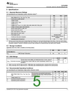
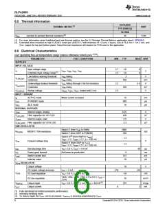
6.5 Thermal Information
DLPA2000
YFF (DSBGA)
56 PINS
THERMAL METRIC(1)
UNIT
RθJA
Junction-to-ambient thermal resistance(2)
45
°C/W
(1) For more information about traditional and new thermal metrics, see the IC Package Thermal Metrics application report, SPRA953.
(2) Estimated when mounted on high K JEDEC board per JESD 51-7 with thickness of 1.6 mm, 4 layers, size of 76.2 mm × 114.3 mm, and
2-oz. copper for top and bottom plane. Actual thermal impedance will depend on PCB used in the application.
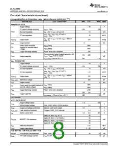
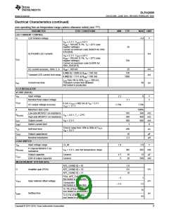
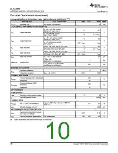
6.6 Electrical Characteristics
over operating free-air temperature range (unless otherwise noted) (see
(1)(2)
)
PARAMETER
TEST CONDITIONS
MIN
TYP
MAX UNIT
SUPPLIES
INPUT VOLTAGE
Input voltage range
2.7
2.3
3.6
3.6
3
6
V
6
VI
VINA, VINR, VINL, VINC
Extended input voltage range(1)
Low-battery warning threshold
Hysteresis
VINA falling
VINA rising
V
VLOW_BAT
100
mV
Undervoltage lockout threshold
Hysteresis
VINA falling (through 5-bit trim function)
VINA rising
2.3
2.5
4.5
V
mV
V
Vhys(UVLO)
VSTARTUP
100
Startup voltage
VBIAS, VOFS, VRST; loaded with 2 mA
INPUT CURRENT
IQ
ACTIVE mode
Motor current excluded
15
900
10
mA
µA
µA
ISTD
IIDLE
STANDBY mode
IDLE mode
INTERNAL SUPPLIES
VV6V
Internal supply, analog
6.25
100
2.5
V
nF
V
CLDO_V6V
VV2V5
Filter capacitor for V6V LDO
Internal supply, logic
CLDO_V2V5 Filter capacitor for V2V5 LDO
2.2
µF
DMD REGULATOR
Switch E (from VINR to SWN)
1000
320
RDS(ON)
MOSFET ON-resistance
Forward voltage drop
mΩ
Switch F (from SWP to PGNDR)
Switch G(2) (from SWP to VBIAS
VINR = 5 V, VSWP = 2 V, IF = 100 mA
)
1.3
1.3
VFW
V
Switch H (from SWP to VOFS
)
VINR = 5 V, VSWP = 2 V, IF = 100 mA
VIN = 2.9 V; COUT = 110 nF
Not tested in production
tDIS
tPG
ILIMIT
L
Rail discharge time
Power-good timeout
Switch current limit
Inductor value
40
µs
ms
mA
µH
6
312
10
VOFS REGULATOR
Output voltage
10
V
DC output voltage accuracy
DC load regulation
IOUT = 2 mA
–2%
2%
VOFS
VIN = 3.6 V, IOUT = 0 to 2 mA
–19
35
V/A
VINA, VINL, VINR, VINC 2.7 to 6.0 V, IOUT
2 mA
=
DC line regulation
mV/V
VRIPPLE
IOUT
Output ripple
VIN = 3.6 V, IOUT = 2 mA, COUT = 440 nF(3)
375
mVpp
mA
Output current
0
3
(1) Fully functional but limited parametric performance
(2) Including rectifying diode
(3) To reduce ripple the COUT can be increased. VRIPPLE is inversely proportional to COUT
.
6
Copyright © 2014–2018, Texas Instruments Incorporated

 TI [ TEXAS INSTRUMENTS ]