DLPA2000
www.ti.com.cn
ZHCSCO5B –JUNE 2014–REVISED FEBRUARY 2018
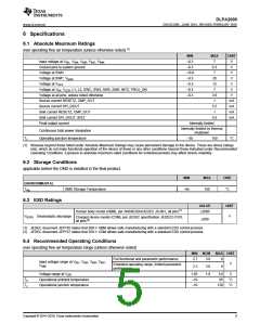
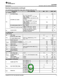
6 Specifications
6.1 Absolute Maximum Ratings
over operating free-air temperature (unless otherwise noted)
(1)
MIN
–0.3
–0.3
–18.0
–0.3
–0.3
–0.3
–0.3
MAX
7
UNIT
V
Input voltage at VINL, VINA, VINR, VINC, VINM
Ground pins to system ground
Voltage at SWN
0.3
7
V
V
Voltage at SWP, VBIAS
20
12
7
V
Voltage at VOFS
V
Voltage at V6V, VLED, L1, L2, SWC, SW4, SW5, SW6, INTZ, PROJ_ON
Voltage at all pins, unless noted otherwise
Source current RESETZ, CMP_OUT
Source current SPI_DOUT
V
3.6
1
V
mA
mA
mA
mA
5.5
1
Sink current RESETZ, CMP_OUT
Sink current SPI_DOUT, INTZ
5.5
Peak output current
Internally limited
Internally limited by thermal
shutdown
Continuous total power dissipation
Operating junction temperature
TJ
–30
150
°C
(1) Stresses beyond those listed under Absolute Maximum Ratings may cause permanent damage to the device. These are stress ratings
only, which do not imply functional operation of the device at these or any other conditions beyond those indicated under Recommended
Operating Conditions. Exposure to absolute-maximum-rated conditions for extended periods may affect device reliability.
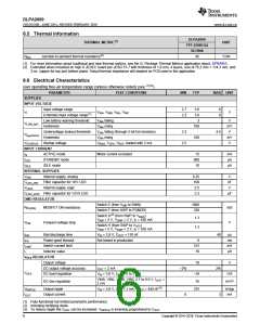
6.2 Storage Conditions
applicable before the DMD is installed in the final product.
MIN
MAX
UNIT
ENVIRONMENTAL
Tstg
DMD Storage Temperature
–65
150
°C
6.3 ESD Ratings
VALUE
UNIT
Human body model (HBM), per ANSI/ESDA/JEDEC JS-001, all pins(1)
±2000
V(ESD) Electrostatic discharge
V
Charged device model (CDM), per JEDEC specification JESD22-C101,
all pins(2)
±500
(1) JEDEC document JEP155 states that 500-V HBM allows safe manufacturing with a standard ESD control process.
(2) JEDEC document JEP157 states that 250-V CDM allows safe manufacturing with a standard ESD control process.
6.4 Recommended Operating Conditions
over operating free-air temperature range (unless otherwise noted)
MIN NOM
MAX UNIT
Full functional and parametric performance
2.7
3.6
3.6
1.8
6
Input voltage range at VINL, VINA, VINR, VINC
VINM
,
V
6
Extended operating range, limited parametric
performance
2.3
Voltage range at VSPI
1.65
–10
–10
3.6
85
V
TA
TJ
Operational ambient temperature
Operational junction temperature
°C
°C
120
Copyright © 2014–2018, Texas Instruments Incorporated
5

 TI [ TEXAS INSTRUMENTS ]