DLPA2000
ZHCSCO5B –JUNE 2014–REVISED FEBRUARY 2018
www.ti.com.cn
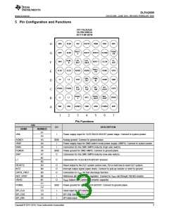
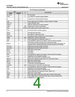
Pin Functions (continued)
PIN
I/O
DESCRIPTION
NAME
SPI_DOUT
VOFS
NUMBER
C6
O
O
SPI data output.
C7
VOFS output rail. Connect to ceramic capacitor.
D1
L2
I
Connection for VLED BUCK-BOOST inductor.
D2
VSPI
D3
I
O
Power supply input for SPI interface. Connect to system I/O voltage.
Analog-comparator output.
CMP_OUT
PWM_IN
AGND
D4
D5
I
Reference voltage input for analog comparator.
Analog ground. Connect to ground plane.
D6
GND
VINA
D7
POWER Power supply input for sensitive analog circuitry.
E1
VLED
O
VLED BUCK-BOOST converter output pin.
E2
SENS1
SENS2
PROJ_ON
DGND
V2V5
E3
I
Input signal from light sensor.
E4
I
I
Input signal from temperature sensor.
E5
Input signal to enable or disable the IC and DLP projector.
Digital ground. Connect to ground plane.
E6
GND
O
E7
Internal supply filter pin for digital logic; typical 2.5 V.
Low-side MOSFET switch for LED cathode. Connect to RGB LED assembly.
Kelvin sense connection to top side of LED current sense resistor.
SW4
F1
O
RLIM_K
F2
I
For best accuracy, route this trace directly to the top of the current sense resistor and
separate it from the normal trace from the current sense resistor to the RLIM pins.
LED_SEL1
LED_SEL0
BOUT1
F3
F4
F5
F6
F7
G1
I
I
Digital input to the RGB STROBE DECODER.
Digital input to the RGB STROBE DECODER.
Motor driver B phase output1.
O
I
LS_IN
Load switch.
LS_OUT
SW5
O
O
Load switch.
Low-side MOSFET switch for LED cathode. Connect to RGB LED assembly.
Connection to LED ‘current sense’ resistor.
Bottom side of sense resistor is connected to GND.
RLIM
G2
O
RBOT_K
AOUT1
BOUT2
VCORE
PGNDCM
SW6
G3
G4
G5
G6
G7
H1
I
O
Kelvin sense connection to ground side of LED current sense resistor.
Motor driver A phase output1.
O
Motor driver B phase output2.
I
VCORE BUCK converter feedback pin.
GND
O
Power ground for VCORE BUCK and motor driver.
Low-side MOSFET switch for LED cathode. Connect to RGB LED assembly.
Connection to LED current sense resistor.
Bottom side of sense resistor is connected to GND.
RLIM
H2
O
V6V
H3
H4
H5
H6
H7
O
O
I
Internal supply filter pin for gate driver circuitry. Typical 6.25 V.
Motor driver A phase output2.
AOUT2
VINM
VINC
SWC
Power supply input for motor driver power stage. Connect to system power.
Power supply input for VCORE BUCK power stage. Connect to system power.
Connection for 1.1-V BUCK inductor.
I
I/O
4
Copyright © 2014–2018, Texas Instruments Incorporated

 TI [ TEXAS INSTRUMENTS ]