DLPA2000
www.ti.com.cn
ZHCSCO5B –JUNE 2014–REVISED FEBRUARY 2018
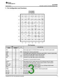
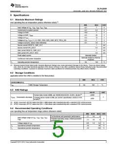
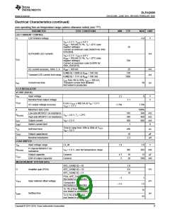
5 Pin Configuration and Functions
YFF PACKAGE
56-PIN DSBGA
BOTTOM VIEW
SW6
SW5
SW4
VLED
L2
RLIM
RLIM
V6V
AOUT2
AOUT1
VINM
VINC
SWC
H
G
F
RBOT_
K
PGND
CM
BOUT2
BOUT1
VCORE
LS_IN
DGND
AGND
RLIM_
K
LED_
SEL1
LED_
SEL0
LS_
OUT
PROJ_
ON
VLED
L2
SENS1
VSPI
SENS2
V2V5
VINA
E
D
C
B
A
CMP_
OUT
PWM_
IN
SPI_
CLK
SPI_
CSZ
SPI_
DIN
SPI_
DOUT
PGNDL
L1
PGNDL
L1
VOFS
VBIAS
SWP
RESET
Z
CNTR_
VRST
REF_
VRST
INTZ
VINR
VINL
VINL
AGND1
SWN
PGNDR
1
2
3
4
5
6
7
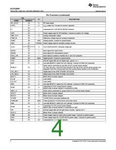
Pin Functions
PIN
I/O
DESCRIPTION
NAME
NUMBER
A1
VINL
I
Power supply input for VLED BUCK-BOOST power stage. Connect to system power.
A2
AGND1
VINR
A3
GND
Analog ground. Connect to ground plane.
A4
I
I
Power supply input for DMD switch mode power supply (SMPS). Connect to system power.
Connection for the DMD SMPS-inductor (high-side switch).
Power ground for DMD SMPS. Connect to ground plane.
Connection for the DMD SMPS-inductor (low-side switch).
SWN
A5
PGNDR
SWP
A6
GND
O
A7
B1
L1
O
Connection for VLED BUCK-BOOST inductor.
B2
RESETZ
INTZ
B3
O
O
O
I
Reset output to the DLP system (active low). Pin is held low to reset DLP system.
Interrupt output signal (open drain). Connect to pull-up resistor or short to ground.
Connection to VRST for fast discharge function.
B4
CNTR_VRST
REF_VRST
VBIAS
B5
B6
Reference pin for the VRST regulator. Connect to VRST rail through 100-kΩ resistor.
VBIAS output rail. Connect to ceramic capacitor.
B7
O
C1
C2
C3
C4
C5
PGNDL
GND
Power ground for VLED BUCK-BOOST. Connect to ground plane.
SPI_CLK
SPI_CSZ
SPI_DIN
I
I
I
Clock input for SPI interface.
SPI chip select (active low).
SPI data input.
Copyright © 2014–2018, Texas Instruments Incorporated
3

 TI [ TEXAS INSTRUMENTS ]