DAC8571
www.ti.com
SLAS373A–DECEMBER 2002–REVISED JULY 2003
•
•
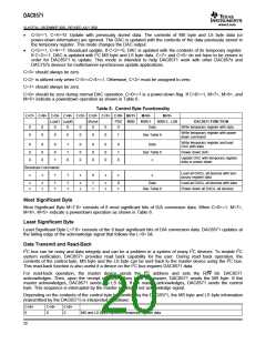
C<5>=1, C<4>=0: Update with previously stored data. The contents of MS byte and LS byte data (or
power-down information) are ignored. The DAC is updated with the contents of the data previously stored in
the temporary register. This mode changes the DAC output.
C<5>=1, C<4>=1: Broadcast update, If C<2>=0, DAC is updated with the contents of its temporary register.
If C<2>=1, DAC is updated with I2C MS byte and LS byte data. C<7> and C<6> do not have to be zeroes in
order for DAC8571 to update. This mode is intended to help DAC8571 work with other DAC857x and
DAC757x devices for multichannel synchronous update applications.
C<3> should always be zero.
C<2> is utilized only when C<5>=C<4>=1. Otherwise, C<2> must be assigned to zero.
C<1> should always be zero.
C<0> should be zero during normal DAC operation. C<0>=1 is a power-down flag. If C<0>=1, M<7>, M<6>, and
M<5> indicate a powerdown operation as shown in Table 6.
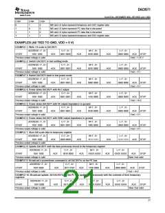
Table 5. Control Byte Functionality
C<7> C<6> C<5> C<4> C<3> C<2> C<1> C<0> M<7>
M<6>
M<5>
Load1 Load0
Brcsel
0
PD0
0
MSB
MSB-1
MSB-2...LSB
DAC8571 FUNCTION
0
0
0
0
0
0
0
0
0
0
Data
Write temporary register with data
Write temporary register with power
down command
0
0
0
1
See Table 6
Write temporary register and load
DAC with data
0
0
0
0
0
0
0
0
1
1
1
0
0
0
0
0
0
0
0
0
0
0
1
0
Data
See Table 6
x
Power down DAC
Update DAC with temporary register
data or power down
Broadcast Commands
Load all DACs, all devices with tem-
porary register data
x
x
1
1
x
0
x
x
x
x
x
x
x
1
1
1
1
x
x
1
1
x
x
0
1
Data
Load all DACs, all devices with data
Power down all DACs, all devices
See Table 6
Most Significant Byte
Most Significant Byte M<7:0> consists of 8 most significant bits of D/A conversion data. When C<0>=1. M<7>,
M<6>, M<5> indicate a powerdown operation as shown in Table 6.
Least Significant Byte
Least Significant Byte L<7:0> consists of the 8 least significant bits of D/A conversion data. DAC8571 updates at
the falling edge of the acknowledge signal that follows the L<0> bit.
Data Transmit and Read-Back
I2C bus can be noisy and data integrity and can be a problem in a system of many I2C devices. To enable I2C
system verification, DAC8571 provides read back capability for the user. During read back operation, the
contents of the control byte, MS byte and the LS byte can be sent back to the master device using the I2C bus.
This read-back function is also useful if a device on the I2C bus inquires DAC8571 data.
For read-back operation, the master device sends the I2C address and sets the R/W bit. DAC8571
acknowledges. Then, upon the receipt of clock pulses from the master, DAC8571 sends the MS byte. If the
master acknowledges, DAC8571 sends the LS byte. If the master acknowledges, DAC8571 sends the control
byte. This sequence is interrupted by the master sending a not acknowledge signal.
Depending on the contents of the control byte transmitted by the DAC8571, the MS byte and LS byte information
(transmitted by the DAC8571) is interpreted as follows:
C<5>
C<4>
C<2>
0
0
0
MS and LS bytes represent temporary register data
20

 TI [ TEXAS INSTRUMENTS ]