DAC8571
www.ti.com
SLAS373A–DECEMBER 2002–REVISED JULY 2003
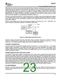
After power-up, the device works in low power mode with its normal power consumption of 170 µA at 5 V. At fast
settling mode, device consumes 250 µA nominally, but settles in 10 µs. For the three power-down modes, the
supply current falls to 200 nA at 5 V (50 nA at 3 V). Not only does the supply current fall but the output stage is
also internally switched from the output of the amplifier to a resistor network of known values. This has the
advantage that the output impedance of the device is known while in power-down mode. There are three
different options: The output is connected internally to GND through a 1-kΩ resistor, a 100-kΩ resistor or it is left
open-circuit (high impedance). The output stage is illustrated in Figure 32.
A power on reset starts the DAC8571 in the low power mode. Low power mode and fast-settling mode settings
stay unchanged during DAC8571 data updates, unless they are specifically overwritten as explained in Table 6.
On the other hand, each new data sequence requiring a DAC update brings the DAC8571 out of the three
power-down conditions.
DAC8571 power settings can be stored in the temporary register, just like data (use C<7:0> = 0000 0001). This
allows simultaneous powerdown capability for multichannel applications.
V
Sense
Amplifier
_
V
OUT
Resistor
String DAC
+
Powerdown
Circuitry
Resistor
Network
Figure 32. Output Stage During Power-Down
All linear circuitry is shut down when the power-down mode is activated. However, the contents of the DAC
register are unaffected when in power-down. The time to exit power-down is typically 2.5 µs for VDD = 5 V and
5 µs for VDD = 3 V. (See the Typical Characteristics section for additional information.)
CURRENT CONSUMPTION
In the low power mode, the DAC8571 typically consumes 170 µA at VDD = 5 V and 150 µA at VDD = 3 V including
reference current consumption. Fast settling mode adds 80 µA of current consumption, but ensures 10-µs
settling. Additional current consumption can occur at the digital inputs if VIH<<VDD. For most efficient power
operation, CMOS logic levels are recommended at the digital inputs to the DAC. In power-down mode, typical
current consumption is 200 nA.
DRIVING RESISTIVE AND CAPACITIVE LOADS
The DAC8571 output stage is capable of driving loads of up to 1000 pF while remaining stable. Within the offset
and gain error margins, the DAC8571 can operate rail-to-rail when driving a capacitive load. Resistive loads of 2
kΩ can be driven by the DAC8571 while achieving a very good load regulation. Load regulation error increases
when the DAC output voltage is close to supply rails. When the outputs of the DAC are driven to the positive rail
under resistive loading, the PMOS transistor of each Class-AB output stage can enter into the linear region.
When this occurs, the added IR voltage drop deteriorates the linearity performance of the DAC. This only occurs
within approximately the top 20 mV of the DAC's digital input-to-voltage output transfer characteristic. The
reference voltage applied to the DAC8571 may be reduced below the supply voltage applied to VDD in order to
eliminate this condition if good linearity is a requirement at full scale (under resistive loading conditions).
AC PERFORMANCE
DAC8571 can achieve typical ac performance of 96-dB signal-to-noise ratio (SNR) and 65-dB total harmonic
distortion (THD), making the DAC8571 a solid choice for applications requiring low SNR at output frequencies at
or below 4 kHz.
23

 TI [ TEXAS INSTRUMENTS ]