DAC8571
www.ti.com
SLAS373A–DECEMBER 2002–REVISED JULY 2003
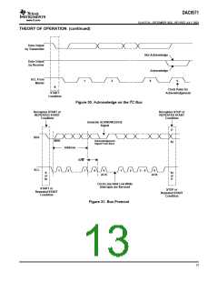
master generates a 9th SCL pulse and monitors the state of the SDA line during the high period of this 9th clock
cycle (master leaves the SDA line high). The SDA line being pulled low by the receiver during the high period of
9th clock cycle is called an acknowledge signal. If the master receives an acknowledge signal, it knows that a
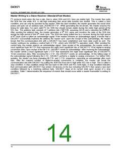
DAC8571 successfully matched the address the master sent. Upon the receipt of this acknowledge, the master
knows that the high-speed communication link with a DAC8571 has been established and more data could be
sent. The master continues by sending a control byte, C<7:0>, which sets DAC8571 operation mode. After
sending the control byte, master expects an acknowledge. Upon the receipt of an acknowledge, the master
sends a most significant byte, M<7:0> that represents the eight most significant bits of DAC8571's 16-bit
digital-to-analog conversion data. Upon the receipt of the M<7:0>, DAC8571 sends an acknowledge. After
receiving the acknowledge, the master sends a least significant byte, L<7:0>, that represents the eight least
significant bits of DAC8571's 16-bit conversion data. After receiving the L<7:0>, the DAC8571 sends an
acknowledge. At the falling edge of the acknowledge signal following the L<0>, DAC8571 performs a digital to
analog conversion, depending on the operational mode. For further DAC updates, the master can keep repeating
M<7:0> and L<7:0> sequences, expecting an acknowledge after each byte. After the required number of digital
to analog conversions is complete, the master can break the communication link with DAC8571 by pulling the
SDA line from low to high while SCL line is high. This is called a stop condition. A stop condition brings the bus
back to idle (SDA and SCL both high). A stop condition indicates that communication with a device (DAC8571)
has ended. All devices on the bus including DAC8571 then await a new start condition followed by a matching
address byte. DAC8571 stays at its current state upon the receipt of a stop condition. A stop condition during the
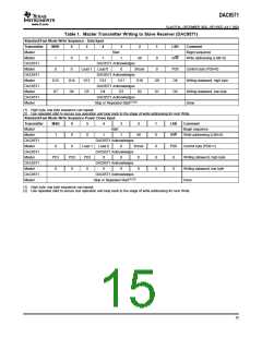
high-speed mode also indicates the end of the high-speed mode. Table 3 demonstrates the sequence of events
that should occur while a master transmitter is writing to DAC8571 in I2C high-speed mode.
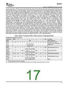
Table 3. Master Transmitter Writes to Slave Receiver in High-Speed Mode
HS Mode Write Sequence-Data Input
Transmitter
Master
MSB
6
5
4
3
2
1
LSB
Comment
Begin sequence(1)
Start
Master
0
0
0
0
1
X
X
X
HS mode master code
No device may acknowledge HS
master code
NONE
Not Acknowledge
Repeated Start
Master
Master
1
0
0
0
0
1
1
A0
Brcsel
D10
D2
0
0
R/W
PD0
D8
Write addressing (LSB = 0)
Control byte (PD0=0)
Writing dataword, high byte
Writing dataword, low byte
Done
DAC8571
Master
DAC8571 Acknowledges
Load 0
DAC8571 Acknowledges
D12 D11
DAC8571 Acknowledges
D4 D3
Load 1
D13
D5
0
DAC8571
Master
D15
D7
D14
D6
D9
D1
DAC8571
Master
D0
DAC8571
Master
DAC8571 Acknowledges
Stop or Repeated Start(2)
(1) High-byte, low-byte sequences can repeat
(2) Use repeated start to secure bus operation and loop back to the stage of write addressing for next Write.
17

 TI [ TEXAS INSTRUMENTS ]