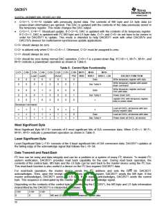
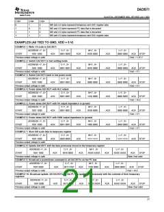
DAC8571
www.ti.com
SLAS373A–DECEMBER 2002–REVISED JULY 2003
OUTPUT VOLTAGE STABILITY
The DAC8571 exhibits excellent temperature stability of 5 ppm/°C typical output voltage drift over the specified
temperature range of the device. This enables the output voltage of each channel to stay within a ±25 µV window
for a ±1°C ambient temperature change. Good power supply rejection ratio (PSRR) performance reduces supply
noise present on VDD from appearing at the outputs to well below 10 µV. Combined with good dc noise
performance and true 16-bit differential linearity, the DAC8571 becomes a perfect choice for closed-loop control
applications.
SETTLING TIME AND OUTPUT GLITCH PERFORMANCE
Settling time to within the 16-bit accurate range of the DAC8571 is achievable within 10 µs for a full-scale code
change at the input. Worst case settling times between consecutive code changes is typically less than 2 µs,
therefore, the update rate is limited by the I2C interface for digital input signals changing code-to-code. For
full-scale output swings, the output stage of each DAC8571 channel typically exhibits less than 100-mV
overshoot and undershoot when driving a 200-pF capacitive load. Code-to-code change glitches are extremely
low (~10µV) given that the code-to-code transition does not cross an Nx4096 code boundary. Due to internal
segmentation of the DAC8571, code-to-code glitches occur at each crossing of an Nx4096 code boundary.
These glitches can approach 100 mVs for N = 15, but settle out within ~2 µs.
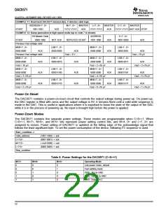
USING REF02 AS A POWER SUPPLY FOR DAC8571
Due to the extremely low supply current required by the DAC8571, a possible configuration is to use a REF02
5-V precision voltage reference to supply the required voltage to the DAC8571's supply input as well as the
reference input, as shown in Figure 33. This is especially useful if the power supply is quite noisy or if the system
supply voltages are at some value other than 5 V. The REF02 outputs a steady supply voltage for the DAC8571.
If the REF02 is used, the current it needs to supply to the DAC8571 is 160-µA typical and 225-µA max for VDD
=
5 V. When a DAC output is loaded, the REF02 also needs to supply the current to the load. The total typical
current required (with a 5-kΩ load on a given DAC output) is:
15 V
5 V
REF02
V
, V
DD ref
2-Wire
l C
Interface
A0
SCL
SDA
V
OUT
= 0 V to 5 V
2
DAC8571
Figure 33. REF02 as a Power Supply
5 V
5 kW
160 mA )
+ 1.16 mA
The load regulation of the REF02 is typically 0.005%/mA, which results in an error of 290 µV for a 1.16-mA
current drawn. This corresponds to a 3.82 LSB error for a 0-V to 5-V output range.
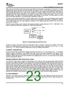
LAYOUT
A precision analog component requires careful layout, adequate bypassing, and clean, well-regulated power
supplies.
The power applied to VDD and VREF should be well regulated and low noise. Switching power supplies and dc/dc
converters often has high-frequency glitches or spikes riding on the output voltage. In addition, digital
components can create similar high-frequency spikes as their internal logic switches states. This noise easily
couples into the DAC output voltage through various paths between the power connections and analog output.
24

 TI [ TEXAS INSTRUMENTS ]