DAC8571
www.ti.com
SLAS373A–DECEMBER 2002–REVISED JULY 2003
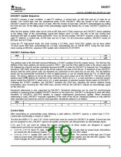
DAC8571 Update Sequence
DAC8571 requires a start condition, a valid I2C address, a control byte, an MS byte and an LS byte for an
update. The control byte sets the operational mode of the DAC8571. After the receipt of the control byte,
DAC8571 expects an MS byte and an LS byte. After the receipt of each byte, DAC8571 acknowledges by pulling
the SDA line low. At the falling edge of the acknowledge signal that follows the LS byte, DAC8571 performs an
update.
After the first update, further data can be sent as MS byte and LS byte sequences and DAC8571 keeps updating
at the falling edge of the acknowledge signal that follows each LS byte. The bits of the last control byte
determine the type of update being performed. Thus, for the first update, DAC8571 requires a start condition, a
valid I2C address, a control byte, an MS byte and an LS byte. For all consecutive updates, DAC8571 needs an
MS byte and an LS byte.
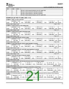
Using the I2C high-speed mode, the clock running a 3.4 MHz, each 16-bit DAC update can be done within
18-clock cycles (MS byte, acknowledge bit, LS byte, acknowledge bit), at 188.88 KSPS. Using the fast mode,
clock running at 400 kHz, maximum DAC update rate is limited to 22.22 KSPS.
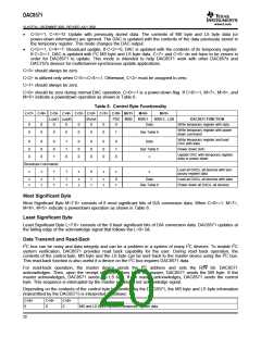
DAC8571 Address Byte
MSB
LSB
1
0
0
1
1
A0
0
R/W
The address byte is the first byte received following a START condition from the master device. The first five bits
(MSBs) of the slave address are factory preset to 10011. The next bit of the address byte is the device select bit
A0, followed by a fixed 0 and the read/write direction bit R/W. In order for DAC8571 to respond, the 7-bit address
should be 10011A00, where the state of the A0 bit matches the state of the A0 pin. A maximum of two DAC8571
devices with the same preset code can therefore be connected on the same bus at one time. The A0 Address
inputs can be permanently connected to VDD or digital ground, or can be actively driven by TTL or CMOS logic
levels. The device address is set by the state of these pins upon power up of the DAC8571. The last bit of the
address byte (R/W) defines the direction of the data flow. When set to a 1, a read operation is selected (master
device reads from DAC8571); when set to a 0, a write operation is selected (master device writes to DAC8571).
Following the START condition, the DAC8571 monitors the SDA bus, checking the device address being
transmitted. Upon receiving the 10011A00 code, and the R/W bit, the DAC8571 outputs an acknowledge signal
on the SDA line.
Broadcast addressing is also supported by DAC8571. Broadcast addressing can be used for synchronously
updating or powering down multiple DAC8571 devices on the same bus. DAC8571 is designed to work with other
members of DAC857x, DAC757x families to support multichannel synchronous update. When broadcast
addressing is used, DAC8571 responds regardless of the state of the A0 pin. Broadcast address is only valid for
write operation and cannot be used for read operation. Broadcast address is as follows.
MSB
LSB
1
0
0
1
0
0
0
0
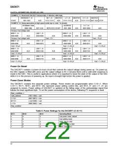
Control Byte
After transmitting an acknowledge pulse following a valid address, DAC8571 expects a control byte C<7:0>.
Control byte functionality is shown in Table 5.
The first two MSBs C<7> and C<6> of the control byte must be zeroes for DAC8571 to update. If these two bits
are not assigned to zero, DAC8571 ignores all update commands, but still generates an acknowledge signal.
C<5> and C<4> are used for setting the update mode. Some of these modes are designed to support
multichannel synchronous operation between multiple devices.
•
C<5>=0, C<4>=0: Store I2C data. The contents of MS byte and LS byte data (or power-down information)
are stored into the temporary register. This mode does not change the DAC output.
C<5>=0, C<4>=1: Update DAC with I2C data. Most common mode. The contents of MS byte and LS byte
data (or power-down information) are stored into the temporary data register and into the DAC register. This
mode changes the DAC output with the contents of I2C MS byte and LS byte data.
•
19

 TI [ TEXAS INSTRUMENTS ]